Home > Press > High, not flat: nanowires for a new chip architecture
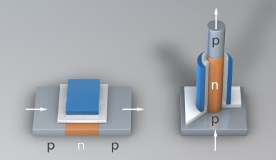 |
| 3D scheme of a usual transistor (left) and of a novel vertical transistor made out of silicon. The arrows symbolize the current flow. Sander M�nster, Dresden. |
Abstract:
Silicon is the most prevalent material in electronics, no matter whether for mobile phones, solar cells or computers. Nanometer-sized wires made of silicon have a large potential for a completely new chip architecture. But this requires a detailed investigation and understanding of their electronic properties which is technologically challenging due to the ultra-small size of the nanowires. Researchers from the Max Planck Institute of Microstructure Physics and the Forschungszentrum Dresden-Rossendorf (FZD) were able to describe the electrical resistance and current flow inside individual silicon nanowires. The results were published in the journal NANO LETTERS.
High, not flat: nanowires for a new chip architecture
Dresden, Germany | Posted on February 2nd, 2010Nowadays, a myriad of silicon transistors are responsible to pass on the information on a microchip. The transistors are arranged in a planar array, i.e. lying flat next to each other, and have shrunk down already to a size of only about 50 nanometers (1 nanometer = 1 millionth part of 1 millimeter). Further miniaturization of transistors with a planar structure will soon come to an end due to fundamental physical limits. Still, even smaller transistors are desirable in order to continuously improve their functions while reducing the cost of the electronics.
Currently, researchers are working hard to find new approaches to overcome the physical limits on downscaling and integration of microchips. One such concept is to fabricate a completely new transistor architecture in three-dimensions. In this concept, instead of arranging them flat on the substrate the silicon transistors are turned by 90 degrees so that they stick out of the chip substrate like tiny columns. In this way, numerous vertical transistors could be built on the area normally occupied by only one planar transistor. This would finally be the step from micro to nanoelectronics.
The fabrication of vertical silicon nanowire arrays has already been reported. Yet there needs to be a more thorough research into the electrical properties of silicon nanowires in order to be able to build reliable transistors for a new generation of microchips. Unlike conventional transistors, the current flow in these column-like transistors will be vertical, and they will be smaller and more energy-saving than today. Last but not least, there are high hopes to fabricate extremely efficient solar cells using silicon nanowires.
The Max Planck researchers in Halle produce monocrystalline silicon nanowires which are particularly suitable as components for microchips. At the FZD's ion beam center, foreign atoms known as �dopants' are implanted into the nanowires. The dopants occupy lattice sites of the host semiconductor increasing the electrical conductivity and the current flow through the semiconductor. Selective implantation of different dopants can change the polarity of the charge carriers in a transistor leading to the switching of the current flow. The planar silicon technology is well developed; however, this is not true for silicon nanostructures. "First, we analyzed wires with a diameter of 100 nanometers and 300 nanometers in length. But what we aim at are wires with a diameter of a few atoms only, as well as wires where individual atoms are strung together. We intend to closely characterize their behavior in materials and want to find out how their electrical properties can be tailored for application in nanoelectronics, e.g. for new field-effect transistors," say FZD physicists Dr. Reinhard Koegler and Dr. Xin Ou.
The nanowires were investigated in Rossendorf using a technique (Scanning Spreading Resistance Microscopy, SSRM) that usually measures the position- dependent electrical resistivity in a specially-prepared two-dimensional cross-section of the nanowire. The resistivity is related to the atomic concentration of the dopants. In the current work, the researchers have found that the dopants in a silicon nanowire, namely boron and phorphorus, do not stay where they are expected, but drift to the surface of the nanowire where they become partially inactive and can no longer contribute to the electrical conductivity. Up until now scientists were lacking an appropriate technique to visualize and quantify the consequences of an unequal distribution of dopants at the nanoscale. Chip designers have to pay attention to the newly found results if nanowires are to be applied for vertical transistors in the future.
Publication:
Xin Ou,�,�,�, Pratyush Das Kanungo,�, Reinhard K�gler,�, Peter Werner,�, Ulrich G�sele,�, Wolfgang Skorupa,�, Xi Wang, �, "Carrier Profiling of Individual Si Nanowires by Scanning Spreading Resistance Microscopy", in: Nano Letters 2010,10,171-175, DOI: 10.1021/nl903228s.
�Max Planck Institute of Microstructure Physics, Halle; � Institute of Ion Beam Physics and Materials Research, FZD; �Shanghai Institute of Microsystem and Information Technology, Chinese Academy of Sciences, Shanghai
####
About Forschungszentrum Dresden-Rossendorf (FZD)
The Forschungszentrum Dresden-Rossendorf, now a member of the Leibniz Association, will become new member of the Helmholtz Association as of January 2011. It is engaged in basic and application-oriented research. The main topics are:
* Advanced Materials Research
* Cancer Research
* Nuclear Safety Research
For more information, please click here
Contacts:
Dr. Wolfgang Skorupa / Dr. Reinhard K�gler
Institute of Ion beam Physics and Materials Research
Forschungszentrum Dresden-Rossendorf
Phone: +49 (0) 351 260 - 3612 / - 3613
Dr. Peter Werner
Max Planck Institute of Microstructure Physics, Halle
Phone: +49 (0) 3455582629
www.mpi-halle.mpg.de/
Contact for the media:
Dr. Christine Bohnet
Press and public relations at FZD
Bautzner Landstr. 400, 01328 Dresden
Phone: +49 (0) 351 260 - 2450 oder 0160 969 288 56
Fax: 0351 260 - 2700
Copyright © Forschungszentrum Dresden-Rossendorf (FZD)
If you have a comment, please Contact us.Issuers of news releases, not 7th Wave, Inc. or Nanotechnology Now, are solely responsible for the accuracy of the content.
Bookmark:


| Related News Press |
News and information
![]() Simulating magnetization in a Heisenberg quantum spin chain April 5th, 2024
Simulating magnetization in a Heisenberg quantum spin chain April 5th, 2024
![]() NRL charters Navy�s quantum inertial navigation path to reduce drift April 5th, 2024
NRL charters Navy�s quantum inertial navigation path to reduce drift April 5th, 2024
![]() Discovery points path to flash-like memory for storing qubits: Rice find could hasten development of nonvolatile quantum memory April 5th, 2024
Discovery points path to flash-like memory for storing qubits: Rice find could hasten development of nonvolatile quantum memory April 5th, 2024
Possible Futures
![]() Discovery points path to flash-like memory for storing qubits: Rice find could hasten development of nonvolatile quantum memory April 5th, 2024
Discovery points path to flash-like memory for storing qubits: Rice find could hasten development of nonvolatile quantum memory April 5th, 2024
![]() With VECSELs towards the quantum internet Fraunhofer: IAF achieves record output power with VECSEL for quantum frequency converters April 5th, 2024
With VECSELs towards the quantum internet Fraunhofer: IAF achieves record output power with VECSEL for quantum frequency converters April 5th, 2024
Chip Technology
![]() Discovery points path to flash-like memory for storing qubits: Rice find could hasten development of nonvolatile quantum memory April 5th, 2024
Discovery points path to flash-like memory for storing qubits: Rice find could hasten development of nonvolatile quantum memory April 5th, 2024
![]() Utilizing palladium for addressing contact issues of buried oxide thin film transistors April 5th, 2024
Utilizing palladium for addressing contact issues of buried oxide thin film transistors April 5th, 2024
![]() HKUST researchers develop new integration technique for efficient coupling of III-V and silicon February 16th, 2024
HKUST researchers develop new integration technique for efficient coupling of III-V and silicon February 16th, 2024
Nanoelectronics
![]() Interdisciplinary: Rice team tackles the future of semiconductors Multiferroics could be the key to ultralow-energy computing October 6th, 2023
Interdisciplinary: Rice team tackles the future of semiconductors Multiferroics could be the key to ultralow-energy computing October 6th, 2023
![]() Key element for a scalable quantum computer: Physicists from Forschungszentrum J�lich and RWTH Aachen University demonstrate electron transport on a quantum chip September 23rd, 2022
Key element for a scalable quantum computer: Physicists from Forschungszentrum J�lich and RWTH Aachen University demonstrate electron transport on a quantum chip September 23rd, 2022
![]() Reduced power consumption in semiconductor devices September 23rd, 2022
Reduced power consumption in semiconductor devices September 23rd, 2022
![]() Atomic level deposition to extend Moore�s law and beyond July 15th, 2022
Atomic level deposition to extend Moore�s law and beyond July 15th, 2022
Announcements
![]() NRL charters Navy�s quantum inertial navigation path to reduce drift April 5th, 2024
NRL charters Navy�s quantum inertial navigation path to reduce drift April 5th, 2024
![]() Discovery points path to flash-like memory for storing qubits: Rice find could hasten development of nonvolatile quantum memory April 5th, 2024
Discovery points path to flash-like memory for storing qubits: Rice find could hasten development of nonvolatile quantum memory April 5th, 2024
Tools
![]() Ferroelectrically modulate the Fermi level of graphene oxide to enhance SERS response November 3rd, 2023
Ferroelectrically modulate the Fermi level of graphene oxide to enhance SERS response November 3rd, 2023
![]() The USTC realizes In situ electron paramagnetic resonance spectroscopy using single nanodiamond sensors November 3rd, 2023
The USTC realizes In situ electron paramagnetic resonance spectroscopy using single nanodiamond sensors November 3rd, 2023
Solar/Photovoltaic
![]() Development of zinc oxide nanopagoda array photoelectrode: photoelectrochemical water-splitting hydrogen production January 12th, 2024
Development of zinc oxide nanopagoda array photoelectrode: photoelectrochemical water-splitting hydrogen production January 12th, 2024
![]() Shedding light on unique conduction mechanisms in a new type of perovskite oxide November 17th, 2023
Shedding light on unique conduction mechanisms in a new type of perovskite oxide November 17th, 2023
![]() Inverted perovskite solar cell breaks 25% efficiency record: Researchers improve cell efficiency using a combination of molecules to address different November 17th, 2023
Inverted perovskite solar cell breaks 25% efficiency record: Researchers improve cell efficiency using a combination of molecules to address different November 17th, 2023
![]() Charged �molecular beasts� the basis for new compounds: Researchers at Leipzig University use �aggressive� fragments of molecular ions for chemical synthesis November 3rd, 2023
Charged �molecular beasts� the basis for new compounds: Researchers at Leipzig University use �aggressive� fragments of molecular ions for chemical synthesis November 3rd, 2023
|
|
||
|
|
||
| The latest news from around the world, FREE | ||
|
|
||
|
|
||
| Premium Products | ||
|
|
||
|
Only the news you want to read!
Learn More |
||
|
|
||
|
Full-service, expert consulting
Learn More |
||
|
|
||