Home > Press > Gecko's lessons transfer well
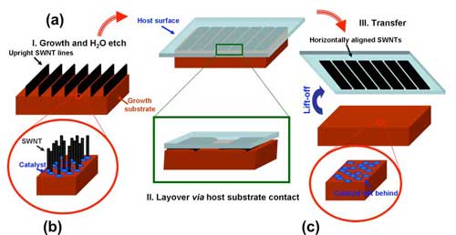 |
| Forests of nanotubes grown via chemical vapor deposition are treated with hydrogen gas and water to loosen their bonds with a catalyst. They can then be transferred to another surface, just like a rubber stamp. |
Abstract:
Dry printing of nanotube patterns to any surface could revolutionize microelectronics and more
Gecko's lessons transfer well
Houston, TX | Posted on January 23rd, 2010Watch a gecko walk up a wall. It defies gravity as it sticks to the surface no matter how smooth it appears to be.
What's happening isn't magic. The gecko stays put because of the electrical attraction - the van der Waals force - between millions of microscopic hairs on its feet and the surface.
The principle applies to new research at Rice University reported this week in the online version of the journal ACS Nano. But in this case, the hairs figuratively come off the gecko and plant themselves on the wall.
Rice graduate student Cary Pint has come up with a way to transfer forests of strongly aligned, single-walled carbon nanotubes (SWNTs) from one surface to another - any surface - in a matter of minutes. The template used to grow the nanotubes, with its catalyst particles still intact, can be used repeatedly to grow more nanotubes, almost like inking a rubber stamp.
Pint is primary author of the research paper, which also details a way to quickly and easily determine the range of diameters in a batch of nanotubes grown through chemical vapor deposition (CVD). Common spectroscopic techniques are poor at seeing tubes bigger than two nanometers in diameter - or most of the nanotubes in the CVD "supergrowth" process.
"This is important since all of the properties of the nanotubes - electrical, thermal and mechanical - change with diameter," he said. "The best thing is that nearly every university has an FTIR (Fourier transform infrared) spectrometer sitting around that can do these measurements, and that should make the process of synthesis and application development from carbon nanotubes much more precise."
Pint and other students and colleagues of Robert Hauge, a Rice distinguished faculty fellow in chemistry, are also investigating ways to take printed films of SWNTs and make them all-conducting or all-semiconducting - a process Hauge refers to as "Fermi-level engineering" for its ability to manipulate electron movement at the nanoscale.
Combined, the techniques represent a huge step toward a nearly limitless number of practical applications that include sensors, highly efficient solar panels and electronic components.
"A big frontier for the field of nanoscience is in finding ways to make what we can do on the nanoscale impact our everyday activities," Hauge said. "For the use of carbon nanotubes in devices that can change the way we do things, a straightforward and scalable way of patterning aligned carbon nanotubes over any surface and in any pattern is a major advance."
Pint said an afternoon of "experimenting with creative ideas" as a first-year graduate student turned into a project that held his interest through his time at Rice. "I realized early on it may be useful to transfer carbon nanotubes to other surfaces," he said.
"I started playing around with water vapor to clean up the amorphous carbons on the nanotubes. When I pulled out a sample, I noticed the nanotubes actually stuck to the tweezers.
"I thought to myself, 'That's really interesting ...'"
Water turns out to be the key. After growing the nanotubes, Pint etches them with a mix of hydrogen gas and water vapor, which weakens the chemical bonds between the tubes and the metal catalyst. When stamped, the nanotubes lie down and adhere, via van der Waals, to the new surface, leaving all traces of the catalyst behind.
Pint, who hopes to defend his dissertation in August, developed a steady enough hand to deposit nanotubes on a range of surfaces - "anything I could lay my hands on" - in patterns that could easily be replicated and certainly enhanced by industrial processes. A striking example of his work is a crisscross film of nanotubes made by stamping one set of lines onto a surface and then reusing the catalyst to grow more tubes and stamping them again over the first pattern at a 90-degree angle. The process took no more than 15 minutes.
"I'll be honest - that was a little bit of luck, combined with the skill of having done this for a few years," he said of the miniature work of art. "But if I were in industry, I would make a machine to do this for me."
Pint believes industries will take a hard look at the technique, which he said could be scaled up easily, for embedding nanotube circuitry into electronic devices.
His own goal is to develop the process to make a range of highly efficient sensing devices. He's also investigating doping techniques that will take the guesswork out of growing metallic (conducting) or semiconducting SWNTs.
Pint and Hauge co-authored the paper with Junichiro Kono, a Rice professor in electrical and computer engineering and in physics and astronomy; Matteo Pasquali, a professor in chemical and biomolecular engineering; former Rice graduate students Ya-Qiong Xu, now an assistant professor of electrical engineering and physics at Vanderbilt University, and Tonya Cherukuri; graduate students Noe Alvarez and Erik Haroz; undergraduate students Sharief Moghazy and Salma Mahzooni; and Stephen Doorn, a researcher at Los Alamos National Laboratory.
The Rice-based Lockheed Martin LANCER program supported the research.
####
For more information, please click here
Contacts:
Jade Boyd
Associate Director /Science Editor
713-348-6778
Copyright © Rice University
If you have a comment, please Contact us.Issuers of news releases, not 7th Wave, Inc. or Nanotechnology Now, are solely responsible for the accuracy of the content.
Bookmark:


| Related News Press |
News and information
![]() Simulating magnetization in a Heisenberg quantum spin chain April 5th, 2024
Simulating magnetization in a Heisenberg quantum spin chain April 5th, 2024
![]() NRL charters Navy�s quantum inertial navigation path to reduce drift April 5th, 2024
NRL charters Navy�s quantum inertial navigation path to reduce drift April 5th, 2024
![]() Discovery points path to flash-like memory for storing qubits: Rice find could hasten development of nonvolatile quantum memory April 5th, 2024
Discovery points path to flash-like memory for storing qubits: Rice find could hasten development of nonvolatile quantum memory April 5th, 2024
Possible Futures
![]() Discovery points path to flash-like memory for storing qubits: Rice find could hasten development of nonvolatile quantum memory April 5th, 2024
Discovery points path to flash-like memory for storing qubits: Rice find could hasten development of nonvolatile quantum memory April 5th, 2024
![]() With VECSELs towards the quantum internet Fraunhofer: IAF achieves record output power with VECSEL for quantum frequency converters April 5th, 2024
With VECSELs towards the quantum internet Fraunhofer: IAF achieves record output power with VECSEL for quantum frequency converters April 5th, 2024
Chip Technology
![]() Discovery points path to flash-like memory for storing qubits: Rice find could hasten development of nonvolatile quantum memory April 5th, 2024
Discovery points path to flash-like memory for storing qubits: Rice find could hasten development of nonvolatile quantum memory April 5th, 2024
![]() Utilizing palladium for addressing contact issues of buried oxide thin film transistors April 5th, 2024
Utilizing palladium for addressing contact issues of buried oxide thin film transistors April 5th, 2024
![]() HKUST researchers develop new integration technique for efficient coupling of III-V and silicon February 16th, 2024
HKUST researchers develop new integration technique for efficient coupling of III-V and silicon February 16th, 2024
Nanotubes/Buckyballs/Fullerenes/Nanorods/Nanostrings
![]() Tests find no free-standing nanotubes released from tire tread wear September 8th, 2023
Tests find no free-standing nanotubes released from tire tread wear September 8th, 2023
![]() Detection of bacteria and viruses with fluorescent nanotubes July 21st, 2023
Detection of bacteria and viruses with fluorescent nanotubes July 21st, 2023
Sensors
Nanoelectronics
![]() Interdisciplinary: Rice team tackles the future of semiconductors Multiferroics could be the key to ultralow-energy computing October 6th, 2023
Interdisciplinary: Rice team tackles the future of semiconductors Multiferroics could be the key to ultralow-energy computing October 6th, 2023
![]() Key element for a scalable quantum computer: Physicists from Forschungszentrum J�lich and RWTH Aachen University demonstrate electron transport on a quantum chip September 23rd, 2022
Key element for a scalable quantum computer: Physicists from Forschungszentrum J�lich and RWTH Aachen University demonstrate electron transport on a quantum chip September 23rd, 2022
![]() Reduced power consumption in semiconductor devices September 23rd, 2022
Reduced power consumption in semiconductor devices September 23rd, 2022
![]() Atomic level deposition to extend Moore�s law and beyond July 15th, 2022
Atomic level deposition to extend Moore�s law and beyond July 15th, 2022
Discoveries
![]() Chemical reactions can scramble quantum information as well as black holes April 5th, 2024
Chemical reactions can scramble quantum information as well as black holes April 5th, 2024
![]() New micromaterial releases nanoparticles that selectively destroy cancer cells April 5th, 2024
New micromaterial releases nanoparticles that selectively destroy cancer cells April 5th, 2024
![]() Utilizing palladium for addressing contact issues of buried oxide thin film transistors April 5th, 2024
Utilizing palladium for addressing contact issues of buried oxide thin film transistors April 5th, 2024
Announcements
![]() NRL charters Navy�s quantum inertial navigation path to reduce drift April 5th, 2024
NRL charters Navy�s quantum inertial navigation path to reduce drift April 5th, 2024
![]() Discovery points path to flash-like memory for storing qubits: Rice find could hasten development of nonvolatile quantum memory April 5th, 2024
Discovery points path to flash-like memory for storing qubits: Rice find could hasten development of nonvolatile quantum memory April 5th, 2024
Solar/Photovoltaic
![]() Development of zinc oxide nanopagoda array photoelectrode: photoelectrochemical water-splitting hydrogen production January 12th, 2024
Development of zinc oxide nanopagoda array photoelectrode: photoelectrochemical water-splitting hydrogen production January 12th, 2024
![]() Shedding light on unique conduction mechanisms in a new type of perovskite oxide November 17th, 2023
Shedding light on unique conduction mechanisms in a new type of perovskite oxide November 17th, 2023
![]() Inverted perovskite solar cell breaks 25% efficiency record: Researchers improve cell efficiency using a combination of molecules to address different November 17th, 2023
Inverted perovskite solar cell breaks 25% efficiency record: Researchers improve cell efficiency using a combination of molecules to address different November 17th, 2023
![]() Charged �molecular beasts� the basis for new compounds: Researchers at Leipzig University use �aggressive� fragments of molecular ions for chemical synthesis November 3rd, 2023
Charged �molecular beasts� the basis for new compounds: Researchers at Leipzig University use �aggressive� fragments of molecular ions for chemical synthesis November 3rd, 2023
|
|
||
|
|
||
| The latest news from around the world, FREE | ||
|
|
||
|
|
||
| Premium Products | ||
|
|
||
|
Only the news you want to read!
Learn More |
||
|
|
||
|
Full-service, expert consulting
Learn More |
||
|
|
||