Home > Press > European collaboration breakthrough in developing graphene
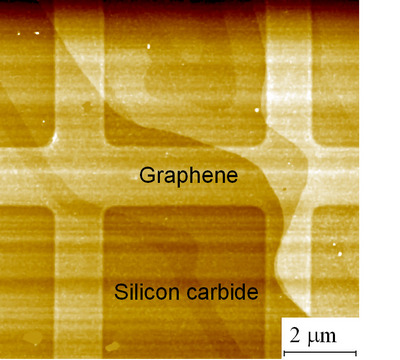 |
| Graphene, only one atom thick, climbs terraces on the surface of a silicone carbide substrate. This picture of a graphene device was taken with an atomic force microscope by NPL's Dr Olga Kazakova |
Abstract:
A collaborative research project has brought the world a step closer to producing a new material on which future nanotechnology could be based. Researchers across Europe, including NPL, have demonstrated how an incredible material, graphene, could hold the key to the future of high-speed electronics, such as micro-chips and touchscreen technology.
European collaboration breakthrough in developing graphene
UK | Posted on January 21st, 2010Graphene has long shown potential, but has previously only been produced on a very small scale, limiting how well it could be measured, understood and developed. A paper published in Nature Nanotechnology explains how researchers have, for the first time, produced graphene to a size and quality where it can be practically developed and successfully measured its electrical characteristics. These significant breakthroughs overcome two of the biggest barriers to scaling up the technology.
A technology for the future
Graphene is a relatively new form of carbon made up of a single layer of atoms arranged in a honeycomb shaped lattice. Despite being one atom thick and chemically simple, graphene is extremely strong and highly conductive, making it ideal for high-speed electronics, photonics and beyond.
Graphene is a strong candidate to replace semiconductor chips. Moore's Law observes that the density of transistors on an integrated circuit doubles every two years, but silicon and other existing transistor materials are thought to be close to the minimum size where they can remain effective. Graphene transistors can potentially run at faster speeds and cope with higher temperatures. Graphene could be the solution to ensuring computing technology to continue to grow in power whilst shrinking in size, extending the life of Moore's law by many years.
Large microchip manufacturers, such as IBM and Intel, have openly expressed interest in the potential of graphene as a material on which future computing could be based.
Graphene also has potential for exciting new innovations such as touchscreen technology, LCD displays and solar cells. Its unparalleled strength and transparency make it perfect for these applications, and its conductivity would offers a dramatic increase in efficiency on existing materials.
Growing to a usable size while maintaining quality
Until now, graphene of sufficient quality has only been produced in the form of small flakes of tiny fractions of a millimeter, using painstaking methods such as peeling layers off graphite crystals with sticky tape. Producing useable electronics requires much larger areas of material to be grown. This project saw researchers, for the first time, produce and successfully operate a large number of electronic devices from a sizable area of graphene layers (approximately 50 mm2).
The graphene sample, was produced epitaxially - a process of growing one crystal layer on another - on silicon carbide. Having such a significant sample not only proves that it can be done in a practical, scalable way, but also allows the scientists to better understand important properties.
Measuring resistance
The second key breakthrough of the project was measuring graphene's electrical characteristics with unprecedented precision, paving the way for convenient and accurate standards to be established. For products such as transistors in computers to work effectively and be commercially viable, manufacturers must be able to make such measurements with incredible accuracy against an agreed international standard.
The international standard for electrical resistance is provided by the Quantum Hall Effect, a phenomenon whereby electrical properties in 2D materials can be determined based only on fundamental constants of nature. The effect has, until now, only been demonstrated with sufficient precision in a small number of conventional semiconductors. Furthermore, such measurements need temperatures close to absolute zero, combined with very strong magnetic fields, and only a few specialised laboratories in the world can achieve these conditions.
Graphene was long tipped to provide an even better standard, but samples were inadequate to prove this. By producing samples of sufficient size and quality, and accurately demonstrate Hall resistance, the team proved that graphene has the potential to supersede conventional semiconductors on a mass scale.
Furthermore, graphene shows the Quantum Hall Effect at much higher temperatures. This means the graphene resistance standard could be used much more widely as more labs can achieve the conditions required for its use. In addition to its advantages of operating speed and durability, this would also speed the production and reduce costs of future electronics technology based on graphene.
NPL's Professor Alexander Tzalenchuk, and the lead author on the Nature Nanotechnology paper, observes:
"It is truly sensational that a large area of epitaxial graphene demonstrated not only structural continuity, but also the degree of perfection required for precise electrical measurements on par with conventional semiconductors with a much longer development history."
Where now?
The research team are hoping to go on to demonstrate even more precise measurement, as well as accurate measurement at even higher temperatures. They are currently seeking EU funding to drive this forward.
Dr JT Janssen, an NPL Fellow who worked on the project, said:
"We've laid the groundwork for the future of graphene production, and will strive in our ongoing research to provide greater understanding of this exciting material. The challenge for industry in the coming years will be to scale the material up in a practical way to meet new technology demands. We have taken a huge step forward, and once the manufacturing processes are in place, we hope graphene will offer the world a faster and cheaper alternative to conventional semiconductors."
The research was a joint project carried by the National Physical Laboratory (UK), Chalmers University of Technology (G�teborg, Sweden), Politecnico di Milano (Italy), Link�ping University (Sweden) and Lancaster University (UK).
Find out more about NPL's research into Quantum Phenomena:
www.npl.co.uk/quantum-phenomena/
For for further information, please contact Alexander Tzalenchuk:
resource.npl.co.uk/expertise/search.php?name=Alexander+Tzalenchuk
####
About National Physical Laboratory
The National Physical Laboratory (NPL) is the UK's National Measurement Institute and is a world-leading centre of excellence in developing and applying the most accurate measurement standards, science and technology.
For more information, please click here
Contacts:
National Physical Laboratory
Hampton Road
Teddington
Middlesex
TW11 0LW
Telephone: +44 20 8977 3222 (Switchboard)
Facsimile: +44 20 8614 0446
Copyright © National Physical Laboratory
If you have a comment, please Contact us.Issuers of news releases, not 7th Wave, Inc. or Nanotechnology Now, are solely responsible for the accuracy of the content.
Bookmark:


| Related News Press |
News and information
![]() Simulating magnetization in a Heisenberg quantum spin chain April 5th, 2024
Simulating magnetization in a Heisenberg quantum spin chain April 5th, 2024
![]() NRL charters Navy�s quantum inertial navigation path to reduce drift April 5th, 2024
NRL charters Navy�s quantum inertial navigation path to reduce drift April 5th, 2024
![]() Discovery points path to flash-like memory for storing qubits: Rice find could hasten development of nonvolatile quantum memory April 5th, 2024
Discovery points path to flash-like memory for storing qubits: Rice find could hasten development of nonvolatile quantum memory April 5th, 2024
![]() Good as gold - improving infectious disease testing with gold nanoparticles April 5th, 2024
Good as gold - improving infectious disease testing with gold nanoparticles April 5th, 2024
Display technology/LEDs/SS Lighting/OLEDs
![]() Utilizing palladium for addressing contact issues of buried oxide thin film transistors April 5th, 2024
Utilizing palladium for addressing contact issues of buried oxide thin film transistors April 5th, 2024
![]() Light guide plate based on perovskite nanocomposites November 3rd, 2023
Light guide plate based on perovskite nanocomposites November 3rd, 2023
![]() Simple ballpoint pen can write custom LEDs August 11th, 2023
Simple ballpoint pen can write custom LEDs August 11th, 2023
Possible Futures
![]() Discovery points path to flash-like memory for storing qubits: Rice find could hasten development of nonvolatile quantum memory April 5th, 2024
Discovery points path to flash-like memory for storing qubits: Rice find could hasten development of nonvolatile quantum memory April 5th, 2024
![]() With VECSELs towards the quantum internet Fraunhofer: IAF achieves record output power with VECSEL for quantum frequency converters April 5th, 2024
With VECSELs towards the quantum internet Fraunhofer: IAF achieves record output power with VECSEL for quantum frequency converters April 5th, 2024
Chip Technology
![]() Discovery points path to flash-like memory for storing qubits: Rice find could hasten development of nonvolatile quantum memory April 5th, 2024
Discovery points path to flash-like memory for storing qubits: Rice find could hasten development of nonvolatile quantum memory April 5th, 2024
![]() Utilizing palladium for addressing contact issues of buried oxide thin film transistors April 5th, 2024
Utilizing palladium for addressing contact issues of buried oxide thin film transistors April 5th, 2024
![]() HKUST researchers develop new integration technique for efficient coupling of III-V and silicon February 16th, 2024
HKUST researchers develop new integration technique for efficient coupling of III-V and silicon February 16th, 2024
Nanoelectronics
![]() Interdisciplinary: Rice team tackles the future of semiconductors Multiferroics could be the key to ultralow-energy computing October 6th, 2023
Interdisciplinary: Rice team tackles the future of semiconductors Multiferroics could be the key to ultralow-energy computing October 6th, 2023
![]() Key element for a scalable quantum computer: Physicists from Forschungszentrum J�lich and RWTH Aachen University demonstrate electron transport on a quantum chip September 23rd, 2022
Key element for a scalable quantum computer: Physicists from Forschungszentrum J�lich and RWTH Aachen University demonstrate electron transport on a quantum chip September 23rd, 2022
![]() Reduced power consumption in semiconductor devices September 23rd, 2022
Reduced power consumption in semiconductor devices September 23rd, 2022
![]() Atomic level deposition to extend Moore�s law and beyond July 15th, 2022
Atomic level deposition to extend Moore�s law and beyond July 15th, 2022
Discoveries
![]() Chemical reactions can scramble quantum information as well as black holes April 5th, 2024
Chemical reactions can scramble quantum information as well as black holes April 5th, 2024
![]() New micromaterial releases nanoparticles that selectively destroy cancer cells April 5th, 2024
New micromaterial releases nanoparticles that selectively destroy cancer cells April 5th, 2024
![]() Utilizing palladium for addressing contact issues of buried oxide thin film transistors April 5th, 2024
Utilizing palladium for addressing contact issues of buried oxide thin film transistors April 5th, 2024
Announcements
![]() NRL charters Navy�s quantum inertial navigation path to reduce drift April 5th, 2024
NRL charters Navy�s quantum inertial navigation path to reduce drift April 5th, 2024
![]() Discovery points path to flash-like memory for storing qubits: Rice find could hasten development of nonvolatile quantum memory April 5th, 2024
Discovery points path to flash-like memory for storing qubits: Rice find could hasten development of nonvolatile quantum memory April 5th, 2024
Alliances/Trade associations/Partnerships/Distributorships
![]() Chicago Quantum Exchange welcomes six new partners highlighting quantum technology solutions, from Chicago and beyond September 23rd, 2022
Chicago Quantum Exchange welcomes six new partners highlighting quantum technology solutions, from Chicago and beyond September 23rd, 2022
![]() University of Illinois Chicago joins Brookhaven Lab's Quantum Center June 10th, 2022
University of Illinois Chicago joins Brookhaven Lab's Quantum Center June 10th, 2022
|
|
||
|
|
||
| The latest news from around the world, FREE | ||
|
|
||
|
|
||
| Premium Products | ||
|
|
||
|
Only the news you want to read!
Learn More |
||
|
|
||
|
Full-service, expert consulting
Learn More |
||
|
|
||