Home > Press > Glitter-sized solar photovoltaics produce competitive results
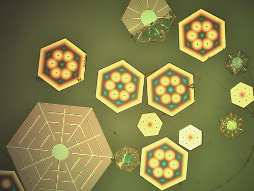 |
| Representative thin crystalline-silicon photovoltaic cells � these are from 14 to 20 micrometers thick and 0.25 to 1 millimeter across. (Image by Murat Okandan) |
Abstract:
Adventures in microsolar supported by microelectronics and MEMS techniques
Glitter-sized solar photovoltaics produce competitive results
Albuquerque, NM | Posted on December 23rd, 2009Sandia National Laboratories scientists have developed tiny glitter-sized photovoltaic cells that could revolutionize the way solar energy is collected and used.
The tiny cells could turn a person into a walking solar battery charger if they were fastened to flexible substrates molded around unusual shapes, such as clothing.
The solar particles, fabricated of crystalline silicon, hold the potential for a variety of new applications. They are expected eventually to be less expensive and have greater efficiencies than current photovoltaic collectors that are pieced together with 6-inch- square solar wafers.
The cells are fabricated using microelectronic and microelectromechanical systems (MEMS) techniques common to today's electronic foundries.
Sandia lead investigator Greg Nielson said the research team has identified more than 20 benefits of scale for its microphotovoltaic cells. These include new applications, improved performance, potential for reduced costs and higher efficiencies.
"Eventually units could be mass-produced and wrapped around unusual shapes for building-integrated solar, tents and maybe even clothing," he said. This would make it possible for hunters, hikers or military personnel in the field to recharge batteries for phones, cameras and other electronic devices as they walk or rest.
Even better, such microengineered panels could have circuits imprinted that would help perform other functions customarily left to large-scale construction with its attendant need for field construction design and permits.
Said Sandia field engineer Vipin Gupta, "Photovoltaic modules made from these microsized cells for the rooftops of homes and warehouses could have intelligent controls, inverters and even storage built in at the chip level. Such an integrated module could greatly simplify the cumbersome design, bid, permit and grid integration process that our solar technical assistance teams see in the field all the time."
For large-scale power generation, said Sandia researcher Murat Okandan, "One of the biggest scale benefits is a significant reduction in manufacturing and installation costs compared with current PV techniques."
Part of the potential cost reduction comes about because microcells require relatively little material to form well-controlled and highly efficient devices.
From 14 to 20 micrometers thick (a human hair is approximately 70 micrometers thick), they are 10 times thinner than conventional 6-inch-by-6-inch brick-sized cells, yet perform at about the same efficiency.
100 times less silicon generates same amount of electricity
"So they use 100 times less silicon to generate the same amount of electricity," said Okandan. "Since they are much smaller and have fewer mechanical deformations for a given environment than the conventional cells, they may also be more reliable over the long term."
Another manufacturing convenience is that the cells, because they are only hundreds of micrometers in diameter, can be fabricated from commercial wafers of any size, including today's 300-millimeter (12-inch) diameter wafers and future 450-millimeter (18-inch) wafers. Further, if one cell proves defective in manufacture, the rest still can be harvested, while if a brick-sized unit goes bad, the entire wafer may be unusable. Also, brick-sized units fabricated larger than the conventional 6-inch-by-6-inch cross section to take advantage of larger wafer size would require thicker power lines to harvest the increased power, creating more cost and possibly shading the wafer. That problem does not exist with the small-cell approach and its individualized wiring.
Other unique features are available because the cells are so small. "The shade tolerance of our units to overhead obstructions is better than conventional PV panels," said Nielson, "because portions of our units not in shade will keep sending out electricity where a partially shaded conventional panel may turn off entirely."
Because flexible substrates can be easily fabricated, high-efficiency PV for ubiquitous solar power becomes more feasible, said Okandan.
A commercial move to microscale PV cells would be a dramatic change from conventional silicon PV modules composed of arrays of 6-inch-by-6-inch wafers. However, by bringing in techniques normally used in MEMS, electronics and the light-emitting diode (LED) industries (for additional work involving gallium arsenide instead of silicon), the change to small cells should be relatively straightforward, Gupta said.
Each cell is formed on silicon wafers, etched and then released inexpensively in hexagonal shapes, with electrical contacts prefabricated on each piece, by borrowing techniques from integrated circuits and MEMS.
Offering a run for their money to conventional large wafers of crystalline silicon, electricity presently can be harvested from the Sandia-created cells with 14.9 percent efficiency. Off-the-shelf commercial modules range from 13 to 20 percent efficient.
A widely used commercial tool called a pick-and-place machine � the current standard for the mass assembly of electronics � can place up to 130,000 pieces of glitter per hour at electrical contact points preestablished on the substrate; the placement takes place at cooler temperatures. The cost is approximately one-tenth of a cent per piece with the number of cells per module determined by the level of optical concentration and the size of the die, likely to be in the 10,000 to 50,000 cell per square meter range. An alternate technology, still at the lab-bench stage, involves self-assembly of the parts at even lower costs.
Solar concentrators � low-cost, prefabricated, optically efficient microlens arrays � can be placed directly over each glitter-sized cell to increase the number of photons arriving to be converted via the photovoltaic effect into electrons. The small cell size means that cheaper and more efficient short focal length microlens arrays can be fabricated for this purpose.
High-voltage output is possible directly from the modules because of the large number of cells in the array. This should reduce costs associated with wiring, due to reduced resistive losses at higher voltages.
Other possible applications for the technology include satellites and remote sensing.
The project combines expertise from Sandia's Microsystems Center; Photovoltaics and Grid Integration Group; the Materials, Devices, and Energy Technologies Group; and the National Renewable Energy Lab's Concentrating Photovoltaics Group.
Involved in the process, in addition to Nielson, Okandan and Gupta, are Jose Luis Cruz-Campa, Paul Resnick, Tammy Pluym, Peggy Clews, Carlos Sanchez, Bill Sweatt, Tony Lentine, Anton Filatov, Mike Sinclair, Mark Overberg, Jeff Nelson, Jennifer Granata, Craig Carmignani, Rick Kemp, Connie Stewart, Jonathan Wierer, George Wang, Jerry Simmons, Jason Strauch, Judith Lavin and Mark Wanlass (NREL).
The work is supported by DOE's Solar Energy Technology Program and Sandia's Laboratory Directed Research & Development program, and has been presented at four technical conferences this year.
The ability of light to produce electrons, and thus electricity, has been known for more than a hundred years.
####
About Sandia National Laboratories
Sandia National Laboratories is a multiprogram laboratory operated by Sandia Corporation, an autonomous Lockheed Martin company, for the U.S. Department of Energy�s National Nuclear Security Administration. With main facilities in Albuquerque, N.M., and Livermore, Calif., Sandia has major R&D responsibilities in national security, energy and environmental technologies, and economic competitiveness.
For more information, please click here
Contacts:
Neal Singer
(505) 845-7078
Copyright © Sandia National Laboratories
If you have a comment, please Contact us.Issuers of news releases, not 7th Wave, Inc. or Nanotechnology Now, are solely responsible for the accuracy of the content.
Bookmark:


| Related News Press |
News and information
![]() Decoding hydrogen‑bond network of electrolyte for cryogenic durable aqueous zinc‑ion batteries January 30th, 2026
Decoding hydrogen‑bond network of electrolyte for cryogenic durable aqueous zinc‑ion batteries January 30th, 2026
![]() COF scaffold membrane with gate‑lane nanostructure for efficient Li+/Mg2+ separation January 30th, 2026
COF scaffold membrane with gate‑lane nanostructure for efficient Li+/Mg2+ separation January 30th, 2026
Possible Futures
![]() Decoding hydrogen‑bond network of electrolyte for cryogenic durable aqueous zinc‑ion batteries January 30th, 2026
Decoding hydrogen‑bond network of electrolyte for cryogenic durable aqueous zinc‑ion batteries January 30th, 2026
![]() COF scaffold membrane with gate‑lane nanostructure for efficient Li+/Mg2+ separation January 30th, 2026
COF scaffold membrane with gate‑lane nanostructure for efficient Li+/Mg2+ separation January 30th, 2026
MEMS
Self Assembly
![]() Diamond glitter: A play of colors with artificial DNA crystals May 17th, 2024
Diamond glitter: A play of colors with artificial DNA crystals May 17th, 2024
![]() Liquid crystal templated chiral nanomaterials October 14th, 2022
Liquid crystal templated chiral nanomaterials October 14th, 2022
![]() Nanoclusters self-organize into centimeter-scale hierarchical assemblies April 22nd, 2022
Nanoclusters self-organize into centimeter-scale hierarchical assemblies April 22nd, 2022
![]() Atom by atom: building precise smaller nanoparticles with templates March 4th, 2022
Atom by atom: building precise smaller nanoparticles with templates March 4th, 2022
Sensors
![]() Tiny nanosheets, big leap: A new sensor detects ethanol at ultra-low levels January 30th, 2026
Tiny nanosheets, big leap: A new sensor detects ethanol at ultra-low levels January 30th, 2026
![]() From sensors to smart systems: the rise of AI-driven photonic noses January 30th, 2026
From sensors to smart systems: the rise of AI-driven photonic noses January 30th, 2026
![]() Sensors innovations for smart lithium-based batteries: advancements, opportunities, and potential challenges August 8th, 2025
Sensors innovations for smart lithium-based batteries: advancements, opportunities, and potential challenges August 8th, 2025
Announcements
![]() Decoding hydrogen‑bond network of electrolyte for cryogenic durable aqueous zinc‑ion batteries January 30th, 2026
Decoding hydrogen‑bond network of electrolyte for cryogenic durable aqueous zinc‑ion batteries January 30th, 2026
![]() COF scaffold membrane with gate‑lane nanostructure for efficient Li+/Mg2+ separation January 30th, 2026
COF scaffold membrane with gate‑lane nanostructure for efficient Li+/Mg2+ separation January 30th, 2026
Military
![]() Quantum engineers �squeeze� laser frequency combs to make more sensitive gas sensors January 17th, 2025
Quantum engineers �squeeze� laser frequency combs to make more sensitive gas sensors January 17th, 2025
![]() Chainmail-like material could be the future of armor: First 2D mechanically interlocked polymer exhibits exceptional flexibility and strength January 17th, 2025
Chainmail-like material could be the future of armor: First 2D mechanically interlocked polymer exhibits exceptional flexibility and strength January 17th, 2025
![]() Single atoms show their true color July 5th, 2024
Single atoms show their true color July 5th, 2024
![]() NRL charters Navy�s quantum inertial navigation path to reduce drift April 5th, 2024
NRL charters Navy�s quantum inertial navigation path to reduce drift April 5th, 2024
Textiles/Clothing
![]() Protective equipment with graphene nanotubes meets the strictest ESD safety standards March 25th, 2022
Protective equipment with graphene nanotubes meets the strictest ESD safety standards March 25th, 2022
![]() Polymer fibers with graphene nanotubes make it possible to heat hard-to-reach, complex-shaped items February 11th, 2022
Polymer fibers with graphene nanotubes make it possible to heat hard-to-reach, complex-shaped items February 11th, 2022
![]() Flexible material shows potential for use in fabrics to heat, cool July 3rd, 2020
Flexible material shows potential for use in fabrics to heat, cool July 3rd, 2020
Aerospace/Space
![]() Decoding hydrogen‑bond network of electrolyte for cryogenic durable aqueous zinc‑ion batteries January 30th, 2026
Decoding hydrogen‑bond network of electrolyte for cryogenic durable aqueous zinc‑ion batteries January 30th, 2026
![]() ICFO researchers overcome long-standing bottleneck in single photon detection with twisted 2D materials August 8th, 2025
ICFO researchers overcome long-standing bottleneck in single photon detection with twisted 2D materials August 8th, 2025
![]() Onion-like nanoparticles found in aircraft exhaust May 14th, 2025
Onion-like nanoparticles found in aircraft exhaust May 14th, 2025
Solar/Photovoltaic
![]() Spinel-type sulfide semiconductors to operate the next-generation LEDs and solar cells For solar-cell absorbers and green-LED source October 3rd, 2025
Spinel-type sulfide semiconductors to operate the next-generation LEDs and solar cells For solar-cell absorbers and green-LED source October 3rd, 2025
![]() KAIST researchers introduce new and improved, next-generation perovskite solar cell November 8th, 2024
KAIST researchers introduce new and improved, next-generation perovskite solar cell November 8th, 2024
![]() Groundbreaking precision in single-molecule optoelectronics August 16th, 2024
Groundbreaking precision in single-molecule optoelectronics August 16th, 2024
![]() Development of zinc oxide nanopagoda array photoelectrode: photoelectrochemical water-splitting hydrogen production January 12th, 2024
Development of zinc oxide nanopagoda array photoelectrode: photoelectrochemical water-splitting hydrogen production January 12th, 2024
|
|
||
|
|
||
| The latest news from around the world, FREE | ||
|
|
||
|
|
||
| Premium Products | ||
|
|
||
|
Only the news you want to read!
Learn More |
||
|
|
||
|
Full-service, expert consulting
Learn More |
||
|
|
||