Home > Press > Measuring Electron Orbitals
 |
| A recent SCIENCE paper sheds a new light on electron density in individual molecular states |
Abstract:
For the first time, it has been possible to measure electron density in individual molecular states using what is known as the photoelectric effect. Now published in SCIENCE, this method represents a key building block in the development of organic semiconductor elements. Supported by the Austrian Science Fund FWF, the success of this project rested on the mathematical transformation of the measured data. This made it possible to interpret the distribution of the electrons and draw conclusions about the potential properties of organic semiconductor elements.
Measuring Electron Orbitals
Austria | Posted on November 16th, 2009Ultra-thin films made of organic molecules form the basis of future semiconductor technologies. Because organic molecules are extremely flexible, they can be used in a whole new range of applications, making it equally possible to create pliable screens and cost-effective solar cells. However, apart from these everyday applications for organic semiconductors, the most important task is to gain a better understanding of the interactions between organic materials and inorganic carrier substances. A team from the Universities of Graz and Leoben has now succeeded in developing a means of doing just that.
Tightly Packed
"The properties of an organic molecule are defined to a large extent by specific electron states", explains Dr. Peter Puschnig of the Chair of Atomistic Modelling and Design of Materials at the University of Leoben, who led the research. He adds: "If we can determine their distribution within the molecule accurately, then we will be able to better understand how organic semiconductor components work and thus increase their efficiency." Until now, there has been a lack of effective methods of measuring this electron distribution. Dr. Puschnig and his team have therefore succeeded in making significant progress.
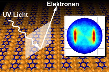
The team's achievement is based on the use of the photoelectric effect. This enables individual electrons to be "knocked out" of organic molecules. As part of this project, an organic molecule was exposed to ultraviolet light that emitted sufficient energy to separate individual electrons from the molecules. The direction and speed of the electrons thus released were then measured using highly-sensitive detectors, generating the basic data required to calculate the electron distribution within the molecule. As part of this process, Prof. Michael Ramsay and his team from the University of Graz used a hexaphenyl film just one molecule thick that had been applied to a copper surface. The team from Graz carried out the actual measurements at the Berliner Elektronen-Speicherring Gesellschaft f�r Synchrotronstrahlung (BESSY, Berlin Electron Storage Ring Society for Synchrotron Radiation).
A Calculated Result
Commenting on the evaluation of this data, Dr. Puschnig says: "It revealed a quite characteristic distribution of the electrons emitted. However, it initially proved difficult to interpret this distribution and it seemed it would be impossible to link the measured data to the original electron distribution in the molecule." It was only by using special mathematical transformations (Fourier Transformation) that the team was able to establish that the measured electron distribution matched that of the molecule. As the distribution was in this instance already known from calculations carried out as part of the density functional theory, it was possible to test and confirm the viability of the new method.
This new method is particularly valuable as it means measuring the behaviour of electrons at the interfaces between organic semiconductors and metals is now relatively easy and highly accurate. The study "Interface controlled and functionalised organic thin films" supported by the FWF as part of the National Research Network (NFN) is thus making a fundamental contribution to future applications of organic semiconductors.
Original publication: Reconstruction of Molecular Orbital Densities from Photoemission Data, P. Puschnig, S. Berkebile, A. J. Fleming, G. Koller, K. Emtsev, T. Seyller, J. D. Riley, C. Ambrosch�Draxl, F. P. Netzer, M. G. Ramsey: Science 326, 702 (2009).
####
About Austrian Science Fund
The Austrian Science Fund (FWF) is Austria's central funding organization for basic research.
The purpose of the FWF is to support the ongoing development of Austrian science and basic research at a high international level. In this way, the FWF makes a significant contribution to cultural development, to the advancement of our knowledge-based society, and thus to the creation of value and wealth in Austria.
For more information, please click here
Contacts:
Scientific contact
Dr. Peter Puschnig
University of Leoben
Chair for Atomistic Modelling and Design of Materials
Austria
T +43 / 3842 / 402 4403
Austrian Science Fund (FWF)
Stefan Bernhardt
Haus der Forschung
Sensengasse 1
1090 Vienna
Austria
T +43 / 1 / 505 67 40 - 8111
Editor/publisher
PR&D - Public Relations for Research & Education
Campus Vienna Biocenter 2
1030 Vienna
Austria
T +43 / 1 / 505 70 44
www.prd.at
Copyright © Austrian Science Fund
If you have a comment, please Contact us.Issuers of news releases, not 7th Wave, Inc. or Nanotechnology Now, are solely responsible for the accuracy of the content.
Bookmark:


| Related News Press |
News and information
![]() Simulating magnetization in a Heisenberg quantum spin chain April 5th, 2024
Simulating magnetization in a Heisenberg quantum spin chain April 5th, 2024
![]() NRL charters Navy�s quantum inertial navigation path to reduce drift April 5th, 2024
NRL charters Navy�s quantum inertial navigation path to reduce drift April 5th, 2024
![]() Discovery points path to flash-like memory for storing qubits: Rice find could hasten development of nonvolatile quantum memory April 5th, 2024
Discovery points path to flash-like memory for storing qubits: Rice find could hasten development of nonvolatile quantum memory April 5th, 2024
![]() Good as gold - improving infectious disease testing with gold nanoparticles April 5th, 2024
Good as gold - improving infectious disease testing with gold nanoparticles April 5th, 2024
Thin films
![]() Utilizing palladium for addressing contact issues of buried oxide thin film transistors April 5th, 2024
Utilizing palladium for addressing contact issues of buried oxide thin film transistors April 5th, 2024
![]() Understanding the mechanism of non-uniform formation of diamond film on tools: Paving the way to a dry process with less environmental impact March 24th, 2023
Understanding the mechanism of non-uniform formation of diamond film on tools: Paving the way to a dry process with less environmental impact March 24th, 2023
![]() New study introduces the best graphite films: The work by Distinguished Professor Feng Ding at UNIST has been published in the October 2022 issue of Nature Nanotechnology November 4th, 2022
New study introduces the best graphite films: The work by Distinguished Professor Feng Ding at UNIST has been published in the October 2022 issue of Nature Nanotechnology November 4th, 2022
Govt.-Legislation/Regulation/Funding/Policy
![]() NRL charters Navy�s quantum inertial navigation path to reduce drift April 5th, 2024
NRL charters Navy�s quantum inertial navigation path to reduce drift April 5th, 2024
![]() Discovery points path to flash-like memory for storing qubits: Rice find could hasten development of nonvolatile quantum memory April 5th, 2024
Discovery points path to flash-like memory for storing qubits: Rice find could hasten development of nonvolatile quantum memory April 5th, 2024
![]() Chemical reactions can scramble quantum information as well as black holes April 5th, 2024
Chemical reactions can scramble quantum information as well as black holes April 5th, 2024
Possible Futures
![]() Discovery points path to flash-like memory for storing qubits: Rice find could hasten development of nonvolatile quantum memory April 5th, 2024
Discovery points path to flash-like memory for storing qubits: Rice find could hasten development of nonvolatile quantum memory April 5th, 2024
![]() With VECSELs towards the quantum internet Fraunhofer: IAF achieves record output power with VECSEL for quantum frequency converters April 5th, 2024
With VECSELs towards the quantum internet Fraunhofer: IAF achieves record output power with VECSEL for quantum frequency converters April 5th, 2024
Chip Technology
![]() Discovery points path to flash-like memory for storing qubits: Rice find could hasten development of nonvolatile quantum memory April 5th, 2024
Discovery points path to flash-like memory for storing qubits: Rice find could hasten development of nonvolatile quantum memory April 5th, 2024
![]() Utilizing palladium for addressing contact issues of buried oxide thin film transistors April 5th, 2024
Utilizing palladium for addressing contact issues of buried oxide thin film transistors April 5th, 2024
![]() HKUST researchers develop new integration technique for efficient coupling of III-V and silicon February 16th, 2024
HKUST researchers develop new integration technique for efficient coupling of III-V and silicon February 16th, 2024
Nanoelectronics
![]() Interdisciplinary: Rice team tackles the future of semiconductors Multiferroics could be the key to ultralow-energy computing October 6th, 2023
Interdisciplinary: Rice team tackles the future of semiconductors Multiferroics could be the key to ultralow-energy computing October 6th, 2023
![]() Key element for a scalable quantum computer: Physicists from Forschungszentrum J�lich and RWTH Aachen University demonstrate electron transport on a quantum chip September 23rd, 2022
Key element for a scalable quantum computer: Physicists from Forschungszentrum J�lich and RWTH Aachen University demonstrate electron transport on a quantum chip September 23rd, 2022
![]() Reduced power consumption in semiconductor devices September 23rd, 2022
Reduced power consumption in semiconductor devices September 23rd, 2022
![]() Atomic level deposition to extend Moore�s law and beyond July 15th, 2022
Atomic level deposition to extend Moore�s law and beyond July 15th, 2022
Announcements
![]() NRL charters Navy�s quantum inertial navigation path to reduce drift April 5th, 2024
NRL charters Navy�s quantum inertial navigation path to reduce drift April 5th, 2024
![]() Discovery points path to flash-like memory for storing qubits: Rice find could hasten development of nonvolatile quantum memory April 5th, 2024
Discovery points path to flash-like memory for storing qubits: Rice find could hasten development of nonvolatile quantum memory April 5th, 2024
Tools
![]() Ferroelectrically modulate the Fermi level of graphene oxide to enhance SERS response November 3rd, 2023
Ferroelectrically modulate the Fermi level of graphene oxide to enhance SERS response November 3rd, 2023
![]() The USTC realizes In situ electron paramagnetic resonance spectroscopy using single nanodiamond sensors November 3rd, 2023
The USTC realizes In situ electron paramagnetic resonance spectroscopy using single nanodiamond sensors November 3rd, 2023
Solar/Photovoltaic
![]() Development of zinc oxide nanopagoda array photoelectrode: photoelectrochemical water-splitting hydrogen production January 12th, 2024
Development of zinc oxide nanopagoda array photoelectrode: photoelectrochemical water-splitting hydrogen production January 12th, 2024
![]() Shedding light on unique conduction mechanisms in a new type of perovskite oxide November 17th, 2023
Shedding light on unique conduction mechanisms in a new type of perovskite oxide November 17th, 2023
![]() Inverted perovskite solar cell breaks 25% efficiency record: Researchers improve cell efficiency using a combination of molecules to address different November 17th, 2023
Inverted perovskite solar cell breaks 25% efficiency record: Researchers improve cell efficiency using a combination of molecules to address different November 17th, 2023
![]() Charged �molecular beasts� the basis for new compounds: Researchers at Leipzig University use �aggressive� fragments of molecular ions for chemical synthesis November 3rd, 2023
Charged �molecular beasts� the basis for new compounds: Researchers at Leipzig University use �aggressive� fragments of molecular ions for chemical synthesis November 3rd, 2023
|
|
||
|
|
||
| The latest news from around the world, FREE | ||
|
|
||
|
|
||
| Premium Products | ||
|
|
||
|
Only the news you want to read!
Learn More |
||
|
|
||
|
Full-service, expert consulting
Learn More |
||
|
|
||