Home > Press > Understanding mechanical properties of silicon nanowires paves way for nanodevices
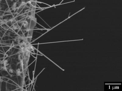 |
| These are silicon nanowires used in the in-situ scanning electron microscopy mechanical testing by Dr. Yong Zhu and his team. Credit: North Carolina State University |
Abstract:
Silicon nanowires are attracting significant attention from the electronics industry due to the drive for ever-smaller electronic devices, from cell phones to computers. The operation of these future devices, and a wide array of additional applications, will depend on the mechanical properties of these nanowires. New research from North Carolina State University shows that silicon nanowires are far more resilient than their larger counterparts, a finding that could pave the way for smaller, sturdier nanoelectronics, nanosensors, light-emitting diodes and other applications.
Understanding mechanical properties of silicon nanowires paves way for nanodevices
Raleigh, NC | Posted on November 12th, 2009It is no surprise that the mechanical properties of silicon nanowires are different from "bulk" - or regular size - silicon materials, because as the diameter of the wires decrease, there is an increasing surface-to-volume ratio. Unfortunately, experimental results reported in the literature on the properties of silicon nanowires have reported conflicting results. So the NC State researchers set out to quantify the elastic and fracture properties of the material.
"The mainstream semiconductor industry is built on silicon," says Dr. Yong Zhu, assistant professor of mechanical engineering at NC State and lead researcher on this project. "These wires are the building blocks for future nanoelectronics." For this study, researchers set out to determine how much abuse these silicon nanowires can take. How do they deform - meaning how much can you stretch or warp the material before it breaks? And how much force can they withstand before they fracture or crack? The researchers focused on nanowires made using the vapor-liquid-solid synthesis process, which is a common way of producing silicon nanowires.
Zhu and his team measured the nanowire properties using in-situ tensile testing inside scanning electron microscopy. A nanomanipulator was used as the actuator and a micro cantilever used as the load sensor. "Our experimental method is direct but simple," says Qingquan Qin, a Ph.D. student at NC State and co-author of the paper. "This method offers real-time observation of nanowire deformation and fracture, while simultaneously providing quantitative stress and strain data. The method is very efficient, so a large number of specimens can be tested within a reasonable period of time."
As it turns out, silicon nanowires deform in a very different way from bulk silicon. "Bulk silicon is very brittle and has limited deformability, meaning that it cannot be stretched or warped very much without breaking." says Feng Xu, a Ph.D. student at NC state and co-author of the paper, "But the silicon nanowires are more resilient, and can sustain much larger deformation. Other properties of silicon nanowires include increasing fracture strength and decreasing elastic modulus as the nanowire gets smaller and smaller."
The fact that silicon nanowires have more deformability and strength is a big deal. "These properties are essential to the design and reliability of novel silicon nanodevices," Zhu says. "The insights gained from this study not only advance fundamental understanding about size effects on mechanical properties of nanostructures, but also give designers more options in designing nanodevices ranging from nanosensors to nanoelectronics to nanostructured solar cells."
###
The study, "Mechanical Properties of Vapor-Liquid-Solid Synthesized Silicon Nanowires," was co-authored by Zhu, Xu, Qin, University of Michigan (UM) researcher Wei Lu and UM Ph.D. student Wayne Fung. The study is published in the Nov. 11 issue of Nano Letters, and was funded by grants from the National Science Foundation and NC State.
####
About North Carolina State University
With more than 31,000 students and nearly 8,000 faculty and staff, North Carolina State University is a comprehensive university known for its leadership in education and research, and globally recognized for its science, technology, engineering and mathematics leadership.
NC State students, faculty and staff are focused. As one of the leading land-grant institutions in the nation, NC State is committed to playing an active and vital role in improving the quality of life for the citizens of North Carolina, the nation and the world.
For more information, please click here
Contacts:
Matt Shipman
919-515-6386
Copyright © Eurekalert
If you have a comment, please Contact us.Issuers of news releases, not 7th Wave, Inc. or Nanotechnology Now, are solely responsible for the accuracy of the content.
Bookmark:


| Related News Press |
News and information
![]() Simulating magnetization in a Heisenberg quantum spin chain April 5th, 2024
Simulating magnetization in a Heisenberg quantum spin chain April 5th, 2024
![]() NRL charters Navy�s quantum inertial navigation path to reduce drift April 5th, 2024
NRL charters Navy�s quantum inertial navigation path to reduce drift April 5th, 2024
![]() Discovery points path to flash-like memory for storing qubits: Rice find could hasten development of nonvolatile quantum memory April 5th, 2024
Discovery points path to flash-like memory for storing qubits: Rice find could hasten development of nonvolatile quantum memory April 5th, 2024
![]() Good as gold - improving infectious disease testing with gold nanoparticles April 5th, 2024
Good as gold - improving infectious disease testing with gold nanoparticles April 5th, 2024
Display technology/LEDs/SS Lighting/OLEDs
![]() Utilizing palladium for addressing contact issues of buried oxide thin film transistors April 5th, 2024
Utilizing palladium for addressing contact issues of buried oxide thin film transistors April 5th, 2024
![]() Light guide plate based on perovskite nanocomposites November 3rd, 2023
Light guide plate based on perovskite nanocomposites November 3rd, 2023
![]() Simple ballpoint pen can write custom LEDs August 11th, 2023
Simple ballpoint pen can write custom LEDs August 11th, 2023
Possible Futures
![]() Discovery points path to flash-like memory for storing qubits: Rice find could hasten development of nonvolatile quantum memory April 5th, 2024
Discovery points path to flash-like memory for storing qubits: Rice find could hasten development of nonvolatile quantum memory April 5th, 2024
![]() With VECSELs towards the quantum internet Fraunhofer: IAF achieves record output power with VECSEL for quantum frequency converters April 5th, 2024
With VECSELs towards the quantum internet Fraunhofer: IAF achieves record output power with VECSEL for quantum frequency converters April 5th, 2024
Chip Technology
![]() Discovery points path to flash-like memory for storing qubits: Rice find could hasten development of nonvolatile quantum memory April 5th, 2024
Discovery points path to flash-like memory for storing qubits: Rice find could hasten development of nonvolatile quantum memory April 5th, 2024
![]() Utilizing palladium for addressing contact issues of buried oxide thin film transistors April 5th, 2024
Utilizing palladium for addressing contact issues of buried oxide thin film transistors April 5th, 2024
![]() HKUST researchers develop new integration technique for efficient coupling of III-V and silicon February 16th, 2024
HKUST researchers develop new integration technique for efficient coupling of III-V and silicon February 16th, 2024
Sensors
Nanoelectronics
![]() Interdisciplinary: Rice team tackles the future of semiconductors Multiferroics could be the key to ultralow-energy computing October 6th, 2023
Interdisciplinary: Rice team tackles the future of semiconductors Multiferroics could be the key to ultralow-energy computing October 6th, 2023
![]() Key element for a scalable quantum computer: Physicists from Forschungszentrum J�lich and RWTH Aachen University demonstrate electron transport on a quantum chip September 23rd, 2022
Key element for a scalable quantum computer: Physicists from Forschungszentrum J�lich and RWTH Aachen University demonstrate electron transport on a quantum chip September 23rd, 2022
![]() Reduced power consumption in semiconductor devices September 23rd, 2022
Reduced power consumption in semiconductor devices September 23rd, 2022
![]() Atomic level deposition to extend Moore�s law and beyond July 15th, 2022
Atomic level deposition to extend Moore�s law and beyond July 15th, 2022
Announcements
![]() NRL charters Navy�s quantum inertial navigation path to reduce drift April 5th, 2024
NRL charters Navy�s quantum inertial navigation path to reduce drift April 5th, 2024
![]() Discovery points path to flash-like memory for storing qubits: Rice find could hasten development of nonvolatile quantum memory April 5th, 2024
Discovery points path to flash-like memory for storing qubits: Rice find could hasten development of nonvolatile quantum memory April 5th, 2024
Photonics/Optics/Lasers
![]() With VECSELs towards the quantum internet Fraunhofer: IAF achieves record output power with VECSEL for quantum frequency converters April 5th, 2024
With VECSELs towards the quantum internet Fraunhofer: IAF achieves record output power with VECSEL for quantum frequency converters April 5th, 2024
![]() Nanoscale CL thermometry with lanthanide-doped heavy-metal oxide in TEM March 8th, 2024
Nanoscale CL thermometry with lanthanide-doped heavy-metal oxide in TEM March 8th, 2024
![]() Optically trapped quantum droplets of light can bind together to form macroscopic complexes March 8th, 2024
Optically trapped quantum droplets of light can bind together to form macroscopic complexes March 8th, 2024
![]() HKUST researchers develop new integration technique for efficient coupling of III-V and silicon February 16th, 2024
HKUST researchers develop new integration technique for efficient coupling of III-V and silicon February 16th, 2024
Solar/Photovoltaic
![]() Development of zinc oxide nanopagoda array photoelectrode: photoelectrochemical water-splitting hydrogen production January 12th, 2024
Development of zinc oxide nanopagoda array photoelectrode: photoelectrochemical water-splitting hydrogen production January 12th, 2024
![]() Shedding light on unique conduction mechanisms in a new type of perovskite oxide November 17th, 2023
Shedding light on unique conduction mechanisms in a new type of perovskite oxide November 17th, 2023
![]() Inverted perovskite solar cell breaks 25% efficiency record: Researchers improve cell efficiency using a combination of molecules to address different November 17th, 2023
Inverted perovskite solar cell breaks 25% efficiency record: Researchers improve cell efficiency using a combination of molecules to address different November 17th, 2023
![]() Charged �molecular beasts� the basis for new compounds: Researchers at Leipzig University use �aggressive� fragments of molecular ions for chemical synthesis November 3rd, 2023
Charged �molecular beasts� the basis for new compounds: Researchers at Leipzig University use �aggressive� fragments of molecular ions for chemical synthesis November 3rd, 2023
|
|
||
|
|
||
| The latest news from around the world, FREE | ||
|
|
||
|
|
||
| Premium Products | ||
|
|
||
|
Only the news you want to read!
Learn More |
||
|
|
||
|
Full-service, expert consulting
Learn More |
||
|
|
||