Home > Press > Quantum Computer Chips Now One Step Closer To Reality
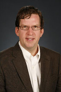 |
| Paul Berger |
Abstract:
In the quest for smaller, faster computer chips, researchers are increasingly turning to quantum mechanics -- the exotic physics of the small.
Quantum Computer Chips Now One Step Closer To Reality
Columbus, OH | Posted on October 16th, 2009The problem: the manufacturing techniques required to make quantum devices have been equally exotic.
That is, until now.
Researchers at Ohio State University have discovered a way to make quantum devices using technology common to the chip-making industry today.
This work might one day enable faster, low-power computer chips. It could also lead to high-resolution cameras for security and public safety, and cameras that provide clear vision through bad weather.
Paul Berger, professor of electrical and computer engineering and professor of physics at Ohio State University, and his colleagues report their findings in an upcoming issue of IEEE Electron Device Letters.
The team fabricated a device called a tunneling diode using the most common chip-making technique, called chemical vapor deposition.
"We wanted to do this using only the tools found in the typical chip-makers toolbox," Berger said. "Here we have a technique that manufacturers could potentially use to fabricate quantum devices directly on a silicon chip, side-by-side with their regular circuits and switches."
The quantum device in question is a resonant interband tunneling diode (RITD) -- a device that enables large amounts of current to be regulated through a circuit, but at very low voltages. That means that such devices run on very little power.
RITDs have been difficult to manufacture because they contain dopants -- chemical elements -- that don't easily fit within a silicon crystal.
Atoms of the RITD dopants antimony or phosphorus, for example, are large compared to atoms of silicon. Because they don't fit into the natural openings inside a silicon crystal, the dopants tend to collect on the surface of a chip.
"It's like when you're playing Tetris and you have a big block raining down, and only a small square to fit it in. The block has to sit on top," Berger said. "When you're building up layers of silicon, these dopants don't readily fit in. Eventually, they clump together on top of the chip."
In the past, researchers have tried adding the dopants while growing the silicon wafer one crystal layer at a time -- using a slow and expensive process called molecular beam epitaxy, a method which is challenging for high-volume manufacturing. That process also creates too many defects within the silicon.
Berger discovered that RITD dopants could be added during chemical vapor deposition, in which a gas carries the chemical elements to the surface of a wafer many layers at a time. The key was determining the right reactor conditions to deliver the dopants to the silicon, he found.
"One key is hydrogen," he said. "It binds to the silicon surface and keeps the dopants from clumping. So you don't have to grow chips at 320 degrees Celsius [approximately 600 degrees Fahrenheit] like you do when using molecular beam epitaxy. You can actually grow them at a higher temperature like 600 degrees Celsius [more than 1100 degrees Fahrenheit] at a lower cost, and with fewer crystal defects."
Tunneling diodes are so named because they exploit a quantum mechanical effect known as tunneling, which lets electrons pass through thin barriers unhindered.
In theory, interband tunneling diodes could form very dense, very efficient micro-circuits in computer chips. A large amount of data could be stored in a small area on a chip with very little energy required.
Researchers judge the usefulness of tunneling diodes by the abrupt change in the current densities they carry, a characteristic known as "peak-to-valley ratio." Different ratios are appropriate for different kinds of devices. Logic circuits such as those on a computer chip are best suited by a ratio of about 2.
The RITDs that Berger's team fabricated had a ratio of 1.85. "We're close, and I'm sure we can do better," he said.
He envisions his RITDs being used for ultra-low-power computer chips operating with small voltages and producing less wasted heat.
"Chip makers today are having a great difficulty boosting performance in each generation, so they pack chips with more and more circuitry, and end up generating a lot of heat," Berger said. "That's why a laptop computer is often too hot to actually sit atop your lap. Soon, their heat output will rival that of a nuclear reactor per unit volume."
"That's why moving to quantum devices will be a game-changer."
RITDs could form high-resolution detectors for imaging devices called focal plane arrays. These arrays operate at wavelengths beyond the human eye and can permit detection of concealed weapons and improvised explosive devices. They can also provide vision through rain, snow, fog, and even mild dust storms, for improved airplane and automobile safety, Berger said. Medical imaging of cancerous tumors is another potential application.
His coauthors on the paper included Si-Young Park, and R. Anisha, both doctoral students in electrical engineering at Ohio State; and Roger Loo, Ngoc Duy Nguyen, Shotaro Takeuchi, and Matty Caymax, all of IMEC, an industrial research center in Belgium.
This work was partially supported by the National Science Foundation.
####
About Ohio State University
The Ohio State University (OSU) is a public research university located in Columbus, Ohio. It was founded in 1870 as a land-grant university and is currently the largest single-campus university in the United States. Ohio State is currently ranked by U.S. News & World Report as the best public university in Ohio, among the top 150 universities in the world, among the top 60 universities in the United States, and among the top 20 public universities in the United States. Ohio State has been officially designated as the flagship institution of the state's public system of higher education by the newly centralized University System of Ohio.
From Wikipedia, the free encyclopedia
For more information, please click here
Contacts:
Paul R. Berger
(614) 247-6235
Written by Pam Frost Gorder
(614) 292-9475
Copyright © Ohio State University
If you have a comment, please Contact us.Issuers of news releases, not 7th Wave, Inc. or Nanotechnology Now, are solely responsible for the accuracy of the content.
Bookmark:


| Related News Press |
News and information
![]() Quantum computer improves AI predictions April 17th, 2026
Quantum computer improves AI predictions April 17th, 2026
![]() Flexible sensor gains sensitivity under pressure April 17th, 2026
Flexible sensor gains sensitivity under pressure April 17th, 2026
![]() A reusable chip for particulate matter sensing April 17th, 2026
A reusable chip for particulate matter sensing April 17th, 2026
![]() Detecting vibrational quantum beating in the predissociation dynamics of SF6 using time-resolved photoelectron spectroscopy April 17th, 2026
Detecting vibrational quantum beating in the predissociation dynamics of SF6 using time-resolved photoelectron spectroscopy April 17th, 2026
Law enforcement/Anti-Counterfeiting/Security/Loss prevention
![]() Chainmail-like material could be the future of armor: First 2D mechanically interlocked polymer exhibits exceptional flexibility and strength January 17th, 2025
Chainmail-like material could be the future of armor: First 2D mechanically interlocked polymer exhibits exceptional flexibility and strength January 17th, 2025
![]() With VECSELs towards the quantum internet Fraunhofer: IAF achieves record output power with VECSEL for quantum frequency converters April 5th, 2024
With VECSELs towards the quantum internet Fraunhofer: IAF achieves record output power with VECSEL for quantum frequency converters April 5th, 2024
![]() Researchers� approach may protect quantum computers from attacks March 8th, 2024
Researchers� approach may protect quantum computers from attacks March 8th, 2024
Govt.-Legislation/Regulation/Funding/Policy
![]() Quantum computer improves AI predictions April 17th, 2026
Quantum computer improves AI predictions April 17th, 2026
![]() Metasurfaces smooth light to boost magnetic sensing precision January 30th, 2026
Metasurfaces smooth light to boost magnetic sensing precision January 30th, 2026
![]() New imaging approach transforms study of bacterial biofilms August 8th, 2025
New imaging approach transforms study of bacterial biofilms August 8th, 2025
Possible Futures
![]() A fundamentally new therapeutic approach to cystic fibrosis: Nanobody repairs cellular defect April 17th, 2026
A fundamentally new therapeutic approach to cystic fibrosis: Nanobody repairs cellular defect April 17th, 2026
![]() UC Irvine physicists discover method to reverse �quantum scrambling� : The work addresses the problem of information loss in quantum computing system April 17th, 2026
UC Irvine physicists discover method to reverse �quantum scrambling� : The work addresses the problem of information loss in quantum computing system April 17th, 2026
Chip Technology
![]() A reusable chip for particulate matter sensing April 17th, 2026
A reusable chip for particulate matter sensing April 17th, 2026
![]() Metasurfaces smooth light to boost magnetic sensing precision January 30th, 2026
Metasurfaces smooth light to boost magnetic sensing precision January 30th, 2026
Quantum Computing
![]() Quantum computer improves AI predictions April 17th, 2026
Quantum computer improves AI predictions April 17th, 2026
![]() UC Irvine physicists discover method to reverse �quantum scrambling� : The work addresses the problem of information loss in quantum computing system April 17th, 2026
UC Irvine physicists discover method to reverse �quantum scrambling� : The work addresses the problem of information loss in quantum computing system April 17th, 2026
![]() Researchers develop molecular qubits that communicate at telecom frequencies October 3rd, 2025
Researchers develop molecular qubits that communicate at telecom frequencies October 3rd, 2025
Nanoelectronics
![]() Lab to industry: InSe wafer-scale breakthrough for future electronics August 8th, 2025
Lab to industry: InSe wafer-scale breakthrough for future electronics August 8th, 2025
![]() Interdisciplinary: Rice team tackles the future of semiconductors Multiferroics could be the key to ultralow-energy computing October 6th, 2023
Interdisciplinary: Rice team tackles the future of semiconductors Multiferroics could be the key to ultralow-energy computing October 6th, 2023
![]() Key element for a scalable quantum computer: Physicists from Forschungszentrum J�lich and RWTH Aachen University demonstrate electron transport on a quantum chip September 23rd, 2022
Key element for a scalable quantum computer: Physicists from Forschungszentrum J�lich and RWTH Aachen University demonstrate electron transport on a quantum chip September 23rd, 2022
![]() Reduced power consumption in semiconductor devices September 23rd, 2022
Reduced power consumption in semiconductor devices September 23rd, 2022
Announcements
![]() A fundamentally new therapeutic approach to cystic fibrosis: Nanobody repairs cellular defect April 17th, 2026
A fundamentally new therapeutic approach to cystic fibrosis: Nanobody repairs cellular defect April 17th, 2026
![]() UC Irvine physicists discover method to reverse �quantum scrambling� : The work addresses the problem of information loss in quantum computing system April 17th, 2026
UC Irvine physicists discover method to reverse �quantum scrambling� : The work addresses the problem of information loss in quantum computing system April 17th, 2026
Homeland Security
![]() The picture of health: Virginia Tech researchers enhance bioimaging and sensing with quantum photonics June 30th, 2023
The picture of health: Virginia Tech researchers enhance bioimaging and sensing with quantum photonics June 30th, 2023
![]() Sensors developed at URI can identify threats at the molecular level: More sensitive than a dog's nose and the sensors don't get tired May 21st, 2021
Sensors developed at URI can identify threats at the molecular level: More sensitive than a dog's nose and the sensors don't get tired May 21st, 2021
![]() Highly sensitive dopamine detector uses 2D materials August 7th, 2020
Highly sensitive dopamine detector uses 2D materials August 7th, 2020
Military
![]() Quantum engineers �squeeze� laser frequency combs to make more sensitive gas sensors January 17th, 2025
Quantum engineers �squeeze� laser frequency combs to make more sensitive gas sensors January 17th, 2025
![]() Chainmail-like material could be the future of armor: First 2D mechanically interlocked polymer exhibits exceptional flexibility and strength January 17th, 2025
Chainmail-like material could be the future of armor: First 2D mechanically interlocked polymer exhibits exceptional flexibility and strength January 17th, 2025
![]() Single atoms show their true color July 5th, 2024
Single atoms show their true color July 5th, 2024
![]() NRL charters Navy�s quantum inertial navigation path to reduce drift April 5th, 2024
NRL charters Navy�s quantum inertial navigation path to reduce drift April 5th, 2024
Quantum nanoscience
![]() Beyond silicon: Electronics at the scale of a single molecule January 30th, 2026
Beyond silicon: Electronics at the scale of a single molecule January 30th, 2026
![]() MXene nanomaterials enter a new dimension Multilayer nanomaterial: MXene flakes created at Drexel University show new promise as 1D scrolls January 30th, 2026
MXene nanomaterials enter a new dimension Multilayer nanomaterial: MXene flakes created at Drexel University show new promise as 1D scrolls January 30th, 2026
![]() ICFO researchers overcome long-standing bottleneck in single photon detection with twisted 2D materials August 8th, 2025
ICFO researchers overcome long-standing bottleneck in single photon detection with twisted 2D materials August 8th, 2025
|
|
||
|
|
||
| The latest news from around the world, FREE | ||
|
|
||
|
|
||
| Premium Products | ||
|
|
||
|
Only the news you want to read!
Learn More |
||
|
|
||
|
Full-service, expert consulting
Learn More |
||
|
|
||