Home > Press > Growth Spurts: Berkeley Lab Researchers Record First Real-Time Direct Observations of Nanocrystal Growth in Solution
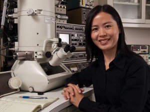 |
| Haimei Zheng is a chemist in the research group of Paul Alivisatos who was the lead author on a Science paper that reports the first ever direct observations in real-time of the growth of single nanocrystals in solution. (Photo by Majed Abolfazli) |
Abstract:
The veil is being lifted from the once unseen world of molecular activity. Not so long ago only the final products were visible and scientists were forced to gauge the processes behind those products by ensemble averages of many molecules.
Growth Spurts: Berkeley Lab Researchers Record First Real-Time Direct Observations of Nanocrystal Growth in Solution
Berkeley, CA | Posted on August 11th, 2009The limitations of that approach have become clear with the advent of technologies that allow for the observation and manipulation of single molecules. A prime example is the recent first ever direct observations in real-time of the growth of single nanocrystals in solution, which revealed that much of what we thought we knew is wrong.
Interim Berkeley Lab Director Paul Alivisatos and Ulrich Dahmen, director of Berkeley Lab's National Center for Electron Microscopy (NCEM), led a team of experts in nanocrystal growth and electron microscopy who combined their skills to observe the dynamic growth of colloidal platinum nanocrystals in solution with subnanometer resolution. Their results showed that while some crystals in solution grow steadily in size via classical nucleation and aggregation - meaning molecules collide and join together - others grow in fits and spurts, driven by "coalescence events," in which small crystals randomly collide and fuse together into larger crystals. Despite their distinctly different growth trajectories, these two processes ultimately yield a nearly monodisperse distribution of nanocrystals, meaning the crystals are all approximately the same size and shape.
"Coalescence events have been previously observed in flask synthesis of colloidal nanocrystals and has been considered detrimental for achieving monodisperse colloidal nanocrystals," says Haimei Zheng, a chemist in Alivisatos' research group, who was the lead author on a paper that reported these results in the journal Science. "In our study, we found that coalescence events are frequently involved in the early stage of nanocrystal growth and yet monodisperse nanocrystals are still formed."
Says Alivisatos, a chemist who holds joint appointments with Berkeley Lab and the University of California at Berkeley where he is the Larry and Diane Bock professor of Nanotechnology, "This direct observation of nanocrystal growth trajectories revealed a set of pathways more complex than those previously envisioned and enables us to re-think the nanocrystal growth mechanism with an eye towards more controlled synthesis."
The Science paper was titled: "Observation of Single Colloidal Platinum Nanocrystal Growth Trajectories." Co-authoring this paper with Zheng, Alivisatos and Dahmen were Rachel Smith, Young-wook Jun and Christian Kisielowski.
Nanocrystals are projected to play important roles in a wide-ranging number of technologies including solar and fuel cell, catalysis, electronics and photonics, medicine, and imaging and sensing. The key to success will be the ability to synthesis nanocrystals with desired physical properties. This will require a much better understanding of colloidal nanocrystal growth mechanisms. While the past two decades have seen tremendous advances in the synthesis of semiconductor, metal and dielectric nanocrystals, these advances have generally been realized through trial and error chemistry. A much more directed and controlled approach to nanocrystal synthesis is needed.
A new technique known as "liquid cell in situ transmission electron microscopy," in which the powerful resolution capabilities of a transmission electron microscope (TEM) are brought to bear on a liquid cell that allows liquids to be observed inside a vacuum, enables the visualization of single nanoparticles in solution. The Berkeley researchers deployed this technique on NCEM's JEOL 3010 In-Situ microscope. Utilizing an electron beam operating at 300 kilovolts of energy, the JEOL 3010 provides outstanding specimen penetration and spatial resolution of about 8 angstroms through the thick liquid cell sample.
"The JEOL 3010 In-Situ Microscope is our best machine for imaging dynamic events, and at 300kV the electron beam has enough penetrating power to maintain high resolution, even when looking through a liquid confined between two thin solid windows," says NCEM director Dahmen. "Our resolution is significantly higher than any previous studies of this nature, which made it possible for us to measure the movement and growth of individual colloidal particles only a few nanometers in size."
Zheng, Dahmen, Alivisatos and their colleagues used the JEOL 3010 and liquid cells microfabricated from a pair of 100-micron-thick silicon wafers with 20 nanometer thick silicon nitride membrane windows to image the growth trajectories of platinum nanocrystals in solution. Platinum nanocrystals are an ideal system for such studies because their high electron contrast allows liquid-cell TEM imaging of individual particles. The JEOL 3010's electron beam was used to both trigger nucleation and drive crystal growth through reduction of the platinum cations.
"Video-rate acquisition allowed us to track nanocrystal growth trajectories from frame-to-frame," says Zheng. "This allowed us to observe that each nanocrystal can either grow steadily through the addition of monomers from solution or by merging with another nanocrystal in random coalescence events."
Zheng says it has been assumed that coalescence events would result in some crystals being much larger than others, a bad thing in that the physical properties of nanocrystals are so dependent upon size and shape that for many applications it is critical that monodispersed nanocrystals be produced during synthesis. Consequently, strategies such as the use of surfactants to coat nanocrystal surfaces have been adopted to avoid coalescence events.
"Our observations provide invaluable direct information on how nanocrystals grow and indicate how we might directly control nanocrystal synthesis for tailored properties," says Zheng. "Also, our in situ liquid cell TEM technique can be applied to other areas of research such as soft matter imaging and nanoparticle catalysis, and offers great potential for addressing many fundamental issues in materials science, chemistry and other fields of science."
Says Dahmen, "From a microscopist's point of view, the ability to observe nanoparticles in liquid solution opens new opportunities in an area that has traditionally been off-limits because electron microscopes require vacuum conditions. We can now see directly what before could only be surmised from the statistical behavior of the ensemble. It's like understanding traffic by watching individual cars instead of listening to the traffic report."
####
About Berkeley Lab
Berkeley Lab is a U.S. Department of Energy national laboratory located in Berkeley, California. It conducts unclassified scientific research for DOE�s Office of Science and is managed by the University of California. Visit our Website at www.lbl.gov/
NCEM is a U.S. Department of Energy national user facility that is hosted at Berkeley Lab. Established in 1983, it stands today as one of the world�s foremost centers for electron microscopy and microcharacterization.
For more information, please click here
Contacts:
Lynn Yarris
(510) 486-5375
Copyright © Berkeley Lab
If you have a comment, please Contact us.Issuers of news releases, not 7th Wave, Inc. or Nanotechnology Now, are solely responsible for the accuracy of the content.
Bookmark:


| Related News Press |
News and information
![]() Simulating magnetization in a Heisenberg quantum spin chain April 5th, 2024
Simulating magnetization in a Heisenberg quantum spin chain April 5th, 2024
![]() NRL charters Navy�s quantum inertial navigation path to reduce drift April 5th, 2024
NRL charters Navy�s quantum inertial navigation path to reduce drift April 5th, 2024
![]() Discovery points path to flash-like memory for storing qubits: Rice find could hasten development of nonvolatile quantum memory April 5th, 2024
Discovery points path to flash-like memory for storing qubits: Rice find could hasten development of nonvolatile quantum memory April 5th, 2024
Nanomedicine
![]() New micromaterial releases nanoparticles that selectively destroy cancer cells April 5th, 2024
New micromaterial releases nanoparticles that selectively destroy cancer cells April 5th, 2024
![]() Good as gold - improving infectious disease testing with gold nanoparticles April 5th, 2024
Good as gold - improving infectious disease testing with gold nanoparticles April 5th, 2024
![]() Researchers develop artificial building blocks of life March 8th, 2024
Researchers develop artificial building blocks of life March 8th, 2024
Sensors
Nanoelectronics
![]() Interdisciplinary: Rice team tackles the future of semiconductors Multiferroics could be the key to ultralow-energy computing October 6th, 2023
Interdisciplinary: Rice team tackles the future of semiconductors Multiferroics could be the key to ultralow-energy computing October 6th, 2023
![]() Key element for a scalable quantum computer: Physicists from Forschungszentrum J�lich and RWTH Aachen University demonstrate electron transport on a quantum chip September 23rd, 2022
Key element for a scalable quantum computer: Physicists from Forschungszentrum J�lich and RWTH Aachen University demonstrate electron transport on a quantum chip September 23rd, 2022
![]() Reduced power consumption in semiconductor devices September 23rd, 2022
Reduced power consumption in semiconductor devices September 23rd, 2022
![]() Atomic level deposition to extend Moore�s law and beyond July 15th, 2022
Atomic level deposition to extend Moore�s law and beyond July 15th, 2022
Announcements
![]() NRL charters Navy�s quantum inertial navigation path to reduce drift April 5th, 2024
NRL charters Navy�s quantum inertial navigation path to reduce drift April 5th, 2024
![]() Discovery points path to flash-like memory for storing qubits: Rice find could hasten development of nonvolatile quantum memory April 5th, 2024
Discovery points path to flash-like memory for storing qubits: Rice find could hasten development of nonvolatile quantum memory April 5th, 2024
Tools
![]() Ferroelectrically modulate the Fermi level of graphene oxide to enhance SERS response November 3rd, 2023
Ferroelectrically modulate the Fermi level of graphene oxide to enhance SERS response November 3rd, 2023
![]() The USTC realizes In situ electron paramagnetic resonance spectroscopy using single nanodiamond sensors November 3rd, 2023
The USTC realizes In situ electron paramagnetic resonance spectroscopy using single nanodiamond sensors November 3rd, 2023
Energy
![]() Development of zinc oxide nanopagoda array photoelectrode: photoelectrochemical water-splitting hydrogen production January 12th, 2024
Development of zinc oxide nanopagoda array photoelectrode: photoelectrochemical water-splitting hydrogen production January 12th, 2024
![]() Shedding light on unique conduction mechanisms in a new type of perovskite oxide November 17th, 2023
Shedding light on unique conduction mechanisms in a new type of perovskite oxide November 17th, 2023
![]() Inverted perovskite solar cell breaks 25% efficiency record: Researchers improve cell efficiency using a combination of molecules to address different November 17th, 2023
Inverted perovskite solar cell breaks 25% efficiency record: Researchers improve cell efficiency using a combination of molecules to address different November 17th, 2023
![]() The efficient perovskite cells with a structured anti-reflective layer � another step towards commercialization on a wider scale October 6th, 2023
The efficient perovskite cells with a structured anti-reflective layer � another step towards commercialization on a wider scale October 6th, 2023
Fuel Cells
![]() Current and Future Developments in Nanomaterials and Carbon Nanotubes: Applications of Nanomaterials in Energy Storage and Electronics October 28th, 2022
Current and Future Developments in Nanomaterials and Carbon Nanotubes: Applications of Nanomaterials in Energy Storage and Electronics October 28th, 2022
Nanobiotechnology
![]() New micromaterial releases nanoparticles that selectively destroy cancer cells April 5th, 2024
New micromaterial releases nanoparticles that selectively destroy cancer cells April 5th, 2024
![]() Good as gold - improving infectious disease testing with gold nanoparticles April 5th, 2024
Good as gold - improving infectious disease testing with gold nanoparticles April 5th, 2024
![]() Researchers develop artificial building blocks of life March 8th, 2024
Researchers develop artificial building blocks of life March 8th, 2024
Photonics/Optics/Lasers
![]() With VECSELs towards the quantum internet Fraunhofer: IAF achieves record output power with VECSEL for quantum frequency converters April 5th, 2024
With VECSELs towards the quantum internet Fraunhofer: IAF achieves record output power with VECSEL for quantum frequency converters April 5th, 2024
![]() Nanoscale CL thermometry with lanthanide-doped heavy-metal oxide in TEM March 8th, 2024
Nanoscale CL thermometry with lanthanide-doped heavy-metal oxide in TEM March 8th, 2024
![]() Optically trapped quantum droplets of light can bind together to form macroscopic complexes March 8th, 2024
Optically trapped quantum droplets of light can bind together to form macroscopic complexes March 8th, 2024
![]() HKUST researchers develop new integration technique for efficient coupling of III-V and silicon February 16th, 2024
HKUST researchers develop new integration technique for efficient coupling of III-V and silicon February 16th, 2024
Solar/Photovoltaic
![]() Development of zinc oxide nanopagoda array photoelectrode: photoelectrochemical water-splitting hydrogen production January 12th, 2024
Development of zinc oxide nanopagoda array photoelectrode: photoelectrochemical water-splitting hydrogen production January 12th, 2024
![]() Shedding light on unique conduction mechanisms in a new type of perovskite oxide November 17th, 2023
Shedding light on unique conduction mechanisms in a new type of perovskite oxide November 17th, 2023
![]() Inverted perovskite solar cell breaks 25% efficiency record: Researchers improve cell efficiency using a combination of molecules to address different November 17th, 2023
Inverted perovskite solar cell breaks 25% efficiency record: Researchers improve cell efficiency using a combination of molecules to address different November 17th, 2023
![]() Charged �molecular beasts� the basis for new compounds: Researchers at Leipzig University use �aggressive� fragments of molecular ions for chemical synthesis November 3rd, 2023
Charged �molecular beasts� the basis for new compounds: Researchers at Leipzig University use �aggressive� fragments of molecular ions for chemical synthesis November 3rd, 2023
|
|
||
|
|
||
| The latest news from around the world, FREE | ||
|
|
||
|
|
||
| Premium Products | ||
|
|
||
|
Only the news you want to read!
Learn More |
||
|
|
||
|
Full-service, expert consulting
Learn More |
||
|
|
||