Home > Press > Sputtering system supports novel commercially-focused silicon device research at Griffith University's microtechnology facility
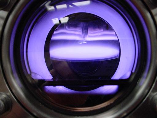 |
| View inside the processing chamber of a Surrey NanoSystems Gamma sputtering system. |
Abstract:
* novel SiC know-how could catalyze breakthrough in non-volatile memory
* flexible system software and quality hardware offers route from research to volume fabrication
Sputtering system supports novel commercially-focused silicon device research at Griffith University's microtechnology facility
Brisbane, Queensland, Australia | Posted on August 3rd, 2009The new Queensland Microtechnology Facility at Griffith University has ordered a Gamma sputtering system from Surrey NanoSystems, to support commercially-backed research into advanced semiconductor devices.
The prime application for the system is to research, develop and establish pilot production procedures for silicon-carbide-on-silicon (SiC-on-Si) devices - on wafers of up to 200 mm diameter. Established with support from the Queensland State Government, Queensland Microtechnology Facility (QMF) has developed a unique epitaxial SiC-on-Si wafer deposition process. By combining the superior semiconductor and physical properties of SiC with low cost silicon wafers, QMF is creating a platform technology that has the potential to enable radical new generations of semiconductor devices - and electronics products.
One of the many performance advantages of SiC is its low leakage, and superior new forms of semiconductor memory for non-volatile and volatile applications are some of the researchers' ambitious targets. The markets for these devices alone are massive: today's Flash memory business alone is worth over $22 billion annually - and the total semiconductor memory market exceeds $60 billion. QMF's memory research and development is funded by Qs Semiconductor Corporation.
A novel SiC-on-Si non-volatile memory cell with a performance exceeding today's commercial criteria has already been demonstrated. QMF's memory cell architecture is very simple and the researchers believe it has the potential to be integrated easily with current silicon fabrication technology - allowing a fast transition into production at 65 nm or smaller node geometries.
Surrey NanoSystems won the competitive tender for three main reasons: the ability of the hardware and its control system to replicate commercial production processes, the flexibility of the system to support wide-ranging research, and the high quality vacuum engineering.
The Gamma sputtering system was specified and chosen by Alan Iacopi, Manager and Deputy Director of the Queensland Microtechnology Facility, whose background includes wafer fabrication experience as a process engineer and more than 15 years in the development of semiconductor production equipment. Surrey NanoSystems' control architecture, which employs a combination of a dedicated real-time PLC controller for the processing hardware with an industrial PC front-end for the user interface, was a big plus point for him compared with the standard PCs used on some other systems. He also liked the system's operating software, GammaSoft, which is purpose designed and provides a simple graphical means of constructing and modifying custom processing 'recipes'.
"We carry out commercially funded projects, and so porting of research into production to minimize time to market is of paramount importance to our investors," says Alan Iacopi. "Gamma was a system I could get excited about as it met the sophisticated design and processing attributes we require to support our wide-ranging research and development goals, including the deposition of complex aluminium interconnect metallization to replicate commercial production processes. The control software was also the most feature-rich of all reviewed."
The superior electrical, thermal, optical and mechanical properties of crystalline SiC make it an interesting material to support progress not only in semiconductor device performance, but also in numerous other emerging technologies. Developing device-quality SiC films on silicon wafers is a very promising means for silicon carbide to enter mainstream electronics markets. The Queensland Microtechnology Facility has some unique ideas for successfully fabricating this materials combination at temperatures low enough for integrated circuit manufacturing, and following its success with non-volatile memory, it is targeting research at a broad range of advanced semiconductor devices and other technologies that could benefit from SiC-on-Si. These include power electronics, solar cells, devices for micro-electro-mechanical systems, and optoelectronics.
The equipment chosen is a configuration of Surrey NanoSystems' Gamma sputtering tool, an advanced PVD (physical vapor deposition) sputtering system that is highly optimized for both performance and versatility of use, and is widely used in R&D and pilot production applications. Capable of deposition over 200 mm diameter wafers or substrates, the system's very high vacuum capability of 5 x 10⁻⁹ Torr, which is as much as two orders of magnitude higher than some other commercially available sputtering systems, provides an exceptionally pure environment to aid uniform film deposition.
Developed and refined over almost 10 years, the company uses a number of novel materials and system building ideas to reduce out-gassing, and enhance the level of cleanliness that can be achieved.
Surrey NanoSystems is also fitting a brand new reactive gas control system - which is believed to be a first for commercial sputtering systems. Instead of a conventional DC pulse controlled process, the Gamma system will use optical emission spectroscopy to dynamically control a high performance gas injection system. Reactive gas control provides a much faster alternative to radio frequency (RF) deposition, combined with comprehensive control over the stoichiometry of the deposited films. The integrated optical emission spectroscopy capability allows users to monitor the process and modify it dynamically - providing the means to avoid the common problem of 'target poisoning'.
More information:
www.griffith.edu.au/engineering-information-technology/queensland-microtechnology-facility
www.surreynanosystems.com
####
About Queensland Microtechnology Facility
The Queensland Microtechnology Facility is a strategic research unit of Griffith University, with support from the Queensland State Government through the Smart State Research Facilities Funding Initiative.
For more information, please click here
Contacts:
Surrey NanoSystems, Euro Business Park, Building 24, Newhaven, BN9 0DQ, UK.
+44 (0)1273 515899;
Contact at the Queensland Microtechnology Facility:
Alan Iacopi
+61 7 3735 4057
Copyright © Wordsun
If you have a comment, please Contact us.Issuers of news releases, not 7th Wave, Inc. or Nanotechnology Now, are solely responsible for the accuracy of the content.
Bookmark:


| Related News Press |
News and information
![]() Simulating magnetization in a Heisenberg quantum spin chain April 5th, 2024
Simulating magnetization in a Heisenberg quantum spin chain April 5th, 2024
![]() NRL charters Navy�s quantum inertial navigation path to reduce drift April 5th, 2024
NRL charters Navy�s quantum inertial navigation path to reduce drift April 5th, 2024
![]() Discovery points path to flash-like memory for storing qubits: Rice find could hasten development of nonvolatile quantum memory April 5th, 2024
Discovery points path to flash-like memory for storing qubits: Rice find could hasten development of nonvolatile quantum memory April 5th, 2024
Chip Technology
![]() Discovery points path to flash-like memory for storing qubits: Rice find could hasten development of nonvolatile quantum memory April 5th, 2024
Discovery points path to flash-like memory for storing qubits: Rice find could hasten development of nonvolatile quantum memory April 5th, 2024
![]() Utilizing palladium for addressing contact issues of buried oxide thin film transistors April 5th, 2024
Utilizing palladium for addressing contact issues of buried oxide thin film transistors April 5th, 2024
![]() HKUST researchers develop new integration technique for efficient coupling of III-V and silicon February 16th, 2024
HKUST researchers develop new integration technique for efficient coupling of III-V and silicon February 16th, 2024
Memory Technology
![]() Utilizing palladium for addressing contact issues of buried oxide thin film transistors April 5th, 2024
Utilizing palladium for addressing contact issues of buried oxide thin film transistors April 5th, 2024
![]() Interdisciplinary: Rice team tackles the future of semiconductors Multiferroics could be the key to ultralow-energy computing October 6th, 2023
Interdisciplinary: Rice team tackles the future of semiconductors Multiferroics could be the key to ultralow-energy computing October 6th, 2023
![]() Researchers discover materials exhibiting huge magnetoresistance June 9th, 2023
Researchers discover materials exhibiting huge magnetoresistance June 9th, 2023
Nanoelectronics
![]() Interdisciplinary: Rice team tackles the future of semiconductors Multiferroics could be the key to ultralow-energy computing October 6th, 2023
Interdisciplinary: Rice team tackles the future of semiconductors Multiferroics could be the key to ultralow-energy computing October 6th, 2023
![]() Key element for a scalable quantum computer: Physicists from Forschungszentrum J�lich and RWTH Aachen University demonstrate electron transport on a quantum chip September 23rd, 2022
Key element for a scalable quantum computer: Physicists from Forschungszentrum J�lich and RWTH Aachen University demonstrate electron transport on a quantum chip September 23rd, 2022
![]() Reduced power consumption in semiconductor devices September 23rd, 2022
Reduced power consumption in semiconductor devices September 23rd, 2022
![]() Atomic level deposition to extend Moore�s law and beyond July 15th, 2022
Atomic level deposition to extend Moore�s law and beyond July 15th, 2022
Announcements
![]() NRL charters Navy�s quantum inertial navigation path to reduce drift April 5th, 2024
NRL charters Navy�s quantum inertial navigation path to reduce drift April 5th, 2024
![]() Discovery points path to flash-like memory for storing qubits: Rice find could hasten development of nonvolatile quantum memory April 5th, 2024
Discovery points path to flash-like memory for storing qubits: Rice find could hasten development of nonvolatile quantum memory April 5th, 2024
Tools
![]() Ferroelectrically modulate the Fermi level of graphene oxide to enhance SERS response November 3rd, 2023
Ferroelectrically modulate the Fermi level of graphene oxide to enhance SERS response November 3rd, 2023
![]() The USTC realizes In situ electron paramagnetic resonance spectroscopy using single nanodiamond sensors November 3rd, 2023
The USTC realizes In situ electron paramagnetic resonance spectroscopy using single nanodiamond sensors November 3rd, 2023
|
|
||
|
|
||
| The latest news from around the world, FREE | ||
|
|
||
|
|
||
| Premium Products | ||
|
|
||
|
Only the news you want to read!
Learn More |
||
|
|
||
|
Full-service, expert consulting
Learn More |
||
|
|
||