Home > Press > USC researchers print dense lattice of transparent nanotube transistors on flexible base
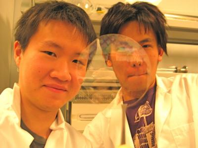 |
| See-through circuit makers: Hsaioh-Kang Chang, left, and Fumiaki Ishikawa, are pictured with their transparent, flexible transistor array.
Credit: USC Viterbi School of Engineering |
Abstract:
Low-temperature process produces both n-type and p-type transistors; allows embedding of LEDs
USC researchers print dense lattice of transparent nanotube transistors on flexible base
Los Angeles, CA | Posted on December 16th, 2008It's a clear, colorless disk about 5 inches in diameter that bends and twists like a playing card, with a lattice of more than 20,000 nanotube transistors capable of high-performance electronics printed upon it using a potentially inexpensive low-temperature process.
Its University of Southern California creators believe the prototype points the way to such long sought after applications as affordable "head-up" car windshield displays. The lattices could also be used to create cheap, ultra thin, low-power "e-paper" displays.
They might even be incorporated into fabric that would change color or pattern as desired for clothing or even wall covering, into nametags, signage and other applications.
A team at the USC Viterbi School of Engineering created the new device, described and illustrated in a just-published paper on "Transparent Electronics Based on Printed Aligned Nanotubes on Rigid and Flexible Structures" in the journal ACS Nano.
Graduate students Fumiaki Ishikawa and Hsiaoh-Kang Chang worked under Professor Chongwu Zhou of the School's Ming Hsieh Department of Electrical Engineering on the project, solving the problems of attaching dense matrices of carbon nanotubes not just to heat-resistant glass but also to flexible but highly heat-vulnerable transparent plastic substrates.
The researchers not only created printed circuit lattices of nanotube-based transistors to the transparent plastic but also additionally connected them to commercial gallium nitrate (GaN) light-emitting diodes, which change their luminosity by a factor of 1,000 as they are energized.
"Our results suggest that aligned nanotubes have great potential to work as building blocks for future transparent electronics," say the researchers.
The thin transparent thin-film transistor technology developed employs carbon nanotubes - tubes with walls one carbon atom thick - as the active channels for the circuits, controlled by iridium-tin oxide electrodes which function as sources, gates and drains.
Earlier attempts at transparent devices used other semiconductor materials with disappointing electronic results, enabling one kind of transistor (n-type); but not p-types; both types are needed for most applications.
The critical improvement in performance, according to the research, came from the ability to produce extremely dense, highly patterned lattices of nanotubes, rather than random tangles and clumps of the material. The Zhou lab has pioneered this technique over the past three years.
The paper contains a description of how the new devices are made.
"These nanotubes were first grown on quartz substrates and then transferred to glass or PET substrates with pre-patterned indium-tin oxide (ITO) gate electrodes, followed by patterning of transparent source and drain electrodes. In contrast to random networked nanotubes, the use of massively aligned nanotubes enabled the devices to exhibit high performance, including high mobility, good transparency, and mechanical flexibility.
"In addition, these aligned nanotube transistors are easy to fabricate and integrate, as compared to individual nanotube devices. The transfer printing process allowed the devices to be fabricated through low temperature process, which is particularly important for realizing transparent electronics on flexible substrates. � While large manufacturability must be addressed before practical applications are considered, our work has paved the way for using aligned nanotubes for high-performance transparent electronics "
Ishikawa and Chang are the principal authors of the paper. Viterbi School graduate students Koungmin Ryu, Pochiang Chen, Alexander Badmaev, Lewis Gomez De Arco, and Guozhen Shen also participated in the project. Zhou, an associate professor, holds the Viterbi School's Jack Munushian Early Career Chair.
The Focus Center Research Program (FCRP FENA) and the National Science Foundation supported the research. The original article can be read at: pubs.acs.org/doi/abs/10.1021/nn800434d
####
For more information, please click here
Contacts:
Eric Mankin
213-821-1887
Copyright © University of Southern California
If you have a comment, please Contact us.Issuers of news releases, not 7th Wave, Inc. or Nanotechnology Now, are solely responsible for the accuracy of the content.
Bookmark:


| Related News Press |
News and information
![]() Simulating magnetization in a Heisenberg quantum spin chain April 5th, 2024
Simulating magnetization in a Heisenberg quantum spin chain April 5th, 2024
![]() NRL charters Navy�s quantum inertial navigation path to reduce drift April 5th, 2024
NRL charters Navy�s quantum inertial navigation path to reduce drift April 5th, 2024
![]() Discovery points path to flash-like memory for storing qubits: Rice find could hasten development of nonvolatile quantum memory April 5th, 2024
Discovery points path to flash-like memory for storing qubits: Rice find could hasten development of nonvolatile quantum memory April 5th, 2024
![]() Good as gold - improving infectious disease testing with gold nanoparticles April 5th, 2024
Good as gold - improving infectious disease testing with gold nanoparticles April 5th, 2024
Display technology/LEDs/SS Lighting/OLEDs
![]() Utilizing palladium for addressing contact issues of buried oxide thin film transistors April 5th, 2024
Utilizing palladium for addressing contact issues of buried oxide thin film transistors April 5th, 2024
![]() Light guide plate based on perovskite nanocomposites November 3rd, 2023
Light guide plate based on perovskite nanocomposites November 3rd, 2023
![]() Simple ballpoint pen can write custom LEDs August 11th, 2023
Simple ballpoint pen can write custom LEDs August 11th, 2023
Chip Technology
![]() Discovery points path to flash-like memory for storing qubits: Rice find could hasten development of nonvolatile quantum memory April 5th, 2024
Discovery points path to flash-like memory for storing qubits: Rice find could hasten development of nonvolatile quantum memory April 5th, 2024
![]() Utilizing palladium for addressing contact issues of buried oxide thin film transistors April 5th, 2024
Utilizing palladium for addressing contact issues of buried oxide thin film transistors April 5th, 2024
![]() HKUST researchers develop new integration technique for efficient coupling of III-V and silicon February 16th, 2024
HKUST researchers develop new integration technique for efficient coupling of III-V and silicon February 16th, 2024
Nanoelectronics
![]() Interdisciplinary: Rice team tackles the future of semiconductors Multiferroics could be the key to ultralow-energy computing October 6th, 2023
Interdisciplinary: Rice team tackles the future of semiconductors Multiferroics could be the key to ultralow-energy computing October 6th, 2023
![]() Key element for a scalable quantum computer: Physicists from Forschungszentrum J�lich and RWTH Aachen University demonstrate electron transport on a quantum chip September 23rd, 2022
Key element for a scalable quantum computer: Physicists from Forschungszentrum J�lich and RWTH Aachen University demonstrate electron transport on a quantum chip September 23rd, 2022
![]() Reduced power consumption in semiconductor devices September 23rd, 2022
Reduced power consumption in semiconductor devices September 23rd, 2022
![]() Atomic level deposition to extend Moore�s law and beyond July 15th, 2022
Atomic level deposition to extend Moore�s law and beyond July 15th, 2022
Discoveries
![]() Chemical reactions can scramble quantum information as well as black holes April 5th, 2024
Chemical reactions can scramble quantum information as well as black holes April 5th, 2024
![]() New micromaterial releases nanoparticles that selectively destroy cancer cells April 5th, 2024
New micromaterial releases nanoparticles that selectively destroy cancer cells April 5th, 2024
![]() Utilizing palladium for addressing contact issues of buried oxide thin film transistors April 5th, 2024
Utilizing palladium for addressing contact issues of buried oxide thin film transistors April 5th, 2024
Announcements
![]() NRL charters Navy�s quantum inertial navigation path to reduce drift April 5th, 2024
NRL charters Navy�s quantum inertial navigation path to reduce drift April 5th, 2024
![]() Discovery points path to flash-like memory for storing qubits: Rice find could hasten development of nonvolatile quantum memory April 5th, 2024
Discovery points path to flash-like memory for storing qubits: Rice find could hasten development of nonvolatile quantum memory April 5th, 2024
Printing/Lithography/Inkjet/Inks/Bio-printing/Dyes
![]() Presenting: Ultrasound-based printing of 3D materials�potentially inside the body December 8th, 2023
Presenting: Ultrasound-based printing of 3D materials�potentially inside the body December 8th, 2023
![]() Simple ballpoint pen can write custom LEDs August 11th, 2023
Simple ballpoint pen can write custom LEDs August 11th, 2023
![]() Disposable electronics on a simple sheet of paper October 7th, 2022
Disposable electronics on a simple sheet of paper October 7th, 2022
|
|
||
|
|
||
| The latest news from around the world, FREE | ||
|
|
||
|
|
||
| Premium Products | ||
|
|
||
|
Only the news you want to read!
Learn More |
||
|
|
||
|
Full-service, expert consulting
Learn More |
||
|
|
||