Home > Press > Researchers show how to measure conductance of carbon nanotubes, one by one
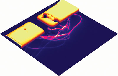 |
| Adam W. Tsen/Provided This 3D microscopic image of a simple nanotube device is taken with photothermal current microscopy performed in Jiwoong Park's lab. The two yellow blocks are electrodes, and strung between them are carbon nanotubes. The strength of each nanotube's electrical signal is visible according to its brightness. |
Abstract:
A single batch of carbon nanotubes -- molecular carbon cylinders that may one day revolutionize electronics engineering -- often includes more than 100 types of tubes, each with different optical and electrical properties. Individual electrical measurements of the molecules typically require such slow and expensive methods as electron-beam lithography.
Researchers show how to measure conductance of carbon nanotubes, one by one
ITHACA, NY | Posted on December 16th, 2008But now a team of Cornell researchers has invented an efficient, inexpensive method to electrically characterize individual carbon nanotubes, even when they are of slightly different shapes and sizes and are networked together.
Led by Jiwoong Park, Cornell assistant professor of chemistry and chemical biology, the group has demonstrated how to measure electrical conductance of both a single nanotube, and up to 150 of them arrayed together, using a single set of electrodes and the heat from a laser. The method is called photothermal current microscopy and could be a major step toward full manipulation of carbon nanotubes in electronic device engineering. It would be especially useful, Park said, for analyzing nanostructures when they are difficult to distinguish from one another.
"There is this tremendous excitement about nanostructures and nanoscale devices," Park said. "But there are a number of things we still need to figure out. One is, we have to be able to measure a large number of them simultaneously so we can have better control when we synthesize them. And that's easier said than done."
The results are reported in Nature Nanotechnology (already online and forthcoming in print Vol. DOI: 10.1038/NNano.2008.363). Collaborators include first author Adam W. Tsen, a graduate student of applied physics; Luke A.K. Donev, a graduate student of physics; Huseyin Kurt, a former postdoctoral associate at Harvard University; and Lihong H. Herman, a graduate student of applied physics.
For their technique, the researchers attached a pair of electrodes to the ends of an array of carbon nanotubes. They then used a laser to heat one nanotube at a time, which reduced the amount of electrical current flowing through it. The conductance change was proportional to the conductance of the nanotube being hit by the laser.
In essence, the nanotubes became temperature sensors, Park explained, and their conductance changes helped the researchers characterize which nanotubes were more or less conductive.
The research is supported by the Air Force Office of Scientific Research and the National Science Foundation.
####
For more information, please click here
Contacts:
Anne Ju
(607) 255-9735
Media Contact:
Blaine Friedlander
(607) 254-8093
Copyright © Cornell University
If you have a comment, please Contact us.Issuers of news releases, not 7th Wave, Inc. or Nanotechnology Now, are solely responsible for the accuracy of the content.
Bookmark:


| Related News Press |
News and information
![]() Simulating magnetization in a Heisenberg quantum spin chain April 5th, 2024
Simulating magnetization in a Heisenberg quantum spin chain April 5th, 2024
![]() NRL charters Navy�s quantum inertial navigation path to reduce drift April 5th, 2024
NRL charters Navy�s quantum inertial navigation path to reduce drift April 5th, 2024
![]() Discovery points path to flash-like memory for storing qubits: Rice find could hasten development of nonvolatile quantum memory April 5th, 2024
Discovery points path to flash-like memory for storing qubits: Rice find could hasten development of nonvolatile quantum memory April 5th, 2024
Govt.-Legislation/Regulation/Funding/Policy
![]() NRL charters Navy�s quantum inertial navigation path to reduce drift April 5th, 2024
NRL charters Navy�s quantum inertial navigation path to reduce drift April 5th, 2024
![]() Discovery points path to flash-like memory for storing qubits: Rice find could hasten development of nonvolatile quantum memory April 5th, 2024
Discovery points path to flash-like memory for storing qubits: Rice find could hasten development of nonvolatile quantum memory April 5th, 2024
![]() Chemical reactions can scramble quantum information as well as black holes April 5th, 2024
Chemical reactions can scramble quantum information as well as black holes April 5th, 2024
Chip Technology
![]() Discovery points path to flash-like memory for storing qubits: Rice find could hasten development of nonvolatile quantum memory April 5th, 2024
Discovery points path to flash-like memory for storing qubits: Rice find could hasten development of nonvolatile quantum memory April 5th, 2024
![]() Utilizing palladium for addressing contact issues of buried oxide thin film transistors April 5th, 2024
Utilizing palladium for addressing contact issues of buried oxide thin film transistors April 5th, 2024
![]() HKUST researchers develop new integration technique for efficient coupling of III-V and silicon February 16th, 2024
HKUST researchers develop new integration technique for efficient coupling of III-V and silicon February 16th, 2024
Nanotubes/Buckyballs/Fullerenes/Nanorods/Nanostrings
![]() Tests find no free-standing nanotubes released from tire tread wear September 8th, 2023
Tests find no free-standing nanotubes released from tire tread wear September 8th, 2023
![]() Detection of bacteria and viruses with fluorescent nanotubes July 21st, 2023
Detection of bacteria and viruses with fluorescent nanotubes July 21st, 2023
Nanoelectronics
![]() Interdisciplinary: Rice team tackles the future of semiconductors Multiferroics could be the key to ultralow-energy computing October 6th, 2023
Interdisciplinary: Rice team tackles the future of semiconductors Multiferroics could be the key to ultralow-energy computing October 6th, 2023
![]() Key element for a scalable quantum computer: Physicists from Forschungszentrum J�lich and RWTH Aachen University demonstrate electron transport on a quantum chip September 23rd, 2022
Key element for a scalable quantum computer: Physicists from Forschungszentrum J�lich and RWTH Aachen University demonstrate electron transport on a quantum chip September 23rd, 2022
![]() Reduced power consumption in semiconductor devices September 23rd, 2022
Reduced power consumption in semiconductor devices September 23rd, 2022
![]() Atomic level deposition to extend Moore�s law and beyond July 15th, 2022
Atomic level deposition to extend Moore�s law and beyond July 15th, 2022
Discoveries
![]() Chemical reactions can scramble quantum information as well as black holes April 5th, 2024
Chemical reactions can scramble quantum information as well as black holes April 5th, 2024
![]() New micromaterial releases nanoparticles that selectively destroy cancer cells April 5th, 2024
New micromaterial releases nanoparticles that selectively destroy cancer cells April 5th, 2024
![]() Utilizing palladium for addressing contact issues of buried oxide thin film transistors April 5th, 2024
Utilizing palladium for addressing contact issues of buried oxide thin film transistors April 5th, 2024
Announcements
![]() NRL charters Navy�s quantum inertial navigation path to reduce drift April 5th, 2024
NRL charters Navy�s quantum inertial navigation path to reduce drift April 5th, 2024
![]() Discovery points path to flash-like memory for storing qubits: Rice find could hasten development of nonvolatile quantum memory April 5th, 2024
Discovery points path to flash-like memory for storing qubits: Rice find could hasten development of nonvolatile quantum memory April 5th, 2024
|
|
||
|
|
||
| The latest news from around the world, FREE | ||
|
|
||
|
|
||
| Premium Products | ||
|
|
||
|
Only the news you want to read!
Learn More |
||
|
|
||
|
Full-service, expert consulting
Learn More |
||
|
|
||