Home > Press > 2D material reshapes 3D electronics for AI hardware
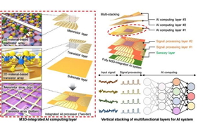 |
| Schematic illustration of an edge computing system based on monolithic 3D-integrated, 2D material-based electronics. The system stacks different functional layers, including AI computing layers, signal-processing layers and a sensory layer, and integrates them into an AI processor. CREDIT Sang-Hoon Bae, McKelvey School of Engineering, Washington University in St. Louis |
Abstract:
Multifunctional computer chips have evolved to do more with integrated sensors, processors, memory and other specialized components. However, as chips have expanded, the time required to move information between functional components has also grown.
2D material reshapes 3D electronics for AI hardware
St. Louis, MO | Posted on December 8th, 2023�Think of it like building a house,� said Sang-Hoon Bae, an assistant professor of mechanical engineering and materials science at the McKelvey School of Engineering at Washington University in St. Louis. �You build out laterally and up vertically to get more function, more room to do more specialized activities, but then you have to spend more time moving or communicating between rooms.�
To address this challenge, Bae and a team of international collaborators, including researchers from the Massachusetts Institute of Technology, Yonsei University, Inha University, Georgia Institute of Technology and the University of Notre Dame, demonstrated monolithic 3D integration of layered 2D material into novel processing hardware for artificial intelligence (AI) computing. They envision that their new approach will not only provide a material-level solution for fully integrating many functions into a single, small electronic chip, but also pave the way for advanced AI computing. Their work was published Nov. 27 in Nature Materials, where it was selected as a front cover article.
The team�s monolithic 3D-integrated chip offers advantages over existing laterally integrated computer chips. The device contains six atomically thin 2D layers, each with its own function, and achieves significantly reduced processing time, power consumption, latency and footprint. This is accomplished through tightly packing the processing layers to ensure dense interlayer connectivity. As a result, the hardware offers unprecedented efficiency and performance in AI computing tasks.
This discovery offers a novel solution to integrate electronics and also opens the door to a new era of multifunctional computing hardware. With ultimate parallelism at its core, this technology could dramatically expand the capabilities of AI systems, enabling them to handle complex tasks with lightning speed and exceptional accuracy, Bae said.
�Monolithic 3D integration has the potential to reshape the entire electronics and computing industry by enabling the development of more compact, powerful and energy-efficient devices,� Bae said. �Atomically thin 2D materials are ideal for this, and my collaborators and I will continue improving this material until we can ultimately integrate all functional layers on a single chip.�
Bae said these devices also are more flexible and functional, making them suitable for more applications.
�From autonomous vehicles to medical diagnostics and data centers, the applications of this monolithic 3D integration technology are potentially boundless,� he said. �For example, in-sensor computing combines sensor and computer functions in one device, instead of a sensor obtaining information then transferring the data to a computer. That lets us obtain a signal and directly compute data resulting in faster processing, less energy consumption and enhanced security because data isn�t being transferred.�
Kang J-H, Shin H, Kim KS, Song M-K, Lee D, Meng Y, Choi C, Suh JM, Kim BJ, Kim H, Hoang AT, Park B-I, Zhou G, Sundaram S, Vuong P, Shin J, Choe J, Xu Z, Younas R, Kim JS, Han S, Lee S, Kim SO, Kang B, Seo S, Ahn H, Seo S, Reidy K, Park E, Mun S, Park M-C, Lee S, Kim H-J, Kum HS, Lin P, Hinkle C, Ougazzaden A, Ahn J-H, Kim J, and Bae S-H. Monolithic 3D integration of 2D materials-based electronics towards ultimate edge computing solutions. Nature Materials. Nov. 27, 2023. DOI: https://doi.org/10.1038/s41563-023-01704-z
This work was supported by Washington University in St. Louis and its Institute of Materials Science & Engineering, the Korea Institute of Science and Technology, the National Research Foundation of Korea, the National Science Foundation, and SUPREME, one of seven centers in JUMP 2.0, a Semiconductor Research Corp. program sponsored by DARPA.
Originally published on the McKelvey School of Engineering website.
####
For more information, please click here
Contacts:
Talia Ogliore
Washington University in St. Louis
Office: 314-935-2919
Copyright © Washington University in St. Louis
If you have a comment, please Contact us.Issuers of news releases, not 7th Wave, Inc. or Nanotechnology Now, are solely responsible for the accuracy of the content.
Bookmark:


| Related Links |
| Related News Press |
News and information
![]() Quantum computer improves AI predictions April 17th, 2026
Quantum computer improves AI predictions April 17th, 2026
![]() Flexible sensor gains sensitivity under pressure April 17th, 2026
Flexible sensor gains sensitivity under pressure April 17th, 2026
![]() A reusable chip for particulate matter sensing April 17th, 2026
A reusable chip for particulate matter sensing April 17th, 2026
![]() Detecting vibrational quantum beating in the predissociation dynamics of SF6 using time-resolved photoelectron spectroscopy April 17th, 2026
Detecting vibrational quantum beating in the predissociation dynamics of SF6 using time-resolved photoelectron spectroscopy April 17th, 2026
2 Dimensional Materials
![]() Flexible sensor gains sensitivity under pressure April 17th, 2026
Flexible sensor gains sensitivity under pressure April 17th, 2026
Govt.-Legislation/Regulation/Funding/Policy
![]() Quantum computer improves AI predictions April 17th, 2026
Quantum computer improves AI predictions April 17th, 2026
![]() Metasurfaces smooth light to boost magnetic sensing precision January 30th, 2026
Metasurfaces smooth light to boost magnetic sensing precision January 30th, 2026
![]() New imaging approach transforms study of bacterial biofilms August 8th, 2025
New imaging approach transforms study of bacterial biofilms August 8th, 2025
Possible Futures
![]() A fundamentally new therapeutic approach to cystic fibrosis: Nanobody repairs cellular defect April 17th, 2026
A fundamentally new therapeutic approach to cystic fibrosis: Nanobody repairs cellular defect April 17th, 2026
![]() UC Irvine physicists discover method to reverse �quantum scrambling� : The work addresses the problem of information loss in quantum computing system April 17th, 2026
UC Irvine physicists discover method to reverse �quantum scrambling� : The work addresses the problem of information loss in quantum computing system April 17th, 2026
Chip Technology
![]() A reusable chip for particulate matter sensing April 17th, 2026
A reusable chip for particulate matter sensing April 17th, 2026
![]() Metasurfaces smooth light to boost magnetic sensing precision January 30th, 2026
Metasurfaces smooth light to boost magnetic sensing precision January 30th, 2026
Discoveries
![]() Quantum computer improves AI predictions April 17th, 2026
Quantum computer improves AI predictions April 17th, 2026
![]() Flexible sensor gains sensitivity under pressure April 17th, 2026
Flexible sensor gains sensitivity under pressure April 17th, 2026
![]() A reusable chip for particulate matter sensing April 17th, 2026
A reusable chip for particulate matter sensing April 17th, 2026
![]() Detecting vibrational quantum beating in the predissociation dynamics of SF6 using time-resolved photoelectron spectroscopy April 17th, 2026
Detecting vibrational quantum beating in the predissociation dynamics of SF6 using time-resolved photoelectron spectroscopy April 17th, 2026
Materials/Metamaterials/Magnetoresistance
![]() First real-time observation of two-dimensional melting process: Researchers at Mainz University unveil new insights into magnetic vortex structures August 8th, 2025
First real-time observation of two-dimensional melting process: Researchers at Mainz University unveil new insights into magnetic vortex structures August 8th, 2025
![]() Researchers unveil a groundbreaking clay-based solution to capture carbon dioxide and combat climate change June 6th, 2025
Researchers unveil a groundbreaking clay-based solution to capture carbon dioxide and combat climate change June 6th, 2025
![]() A 1960s idea inspires NBI researchers to study hitherto inaccessible quantum states June 6th, 2025
A 1960s idea inspires NBI researchers to study hitherto inaccessible quantum states June 6th, 2025
![]() Institute for Nanoscience hosts annual proposal planning meeting May 16th, 2025
Institute for Nanoscience hosts annual proposal planning meeting May 16th, 2025
Announcements
![]() A fundamentally new therapeutic approach to cystic fibrosis: Nanobody repairs cellular defect April 17th, 2026
A fundamentally new therapeutic approach to cystic fibrosis: Nanobody repairs cellular defect April 17th, 2026
![]() UC Irvine physicists discover method to reverse �quantum scrambling� : The work addresses the problem of information loss in quantum computing system April 17th, 2026
UC Irvine physicists discover method to reverse �quantum scrambling� : The work addresses the problem of information loss in quantum computing system April 17th, 2026
Interviews/Book Reviews/Essays/Reports/Podcasts/Journals/White papers/Posters
![]() A fundamentally new therapeutic approach to cystic fibrosis: Nanobody repairs cellular defect April 17th, 2026
A fundamentally new therapeutic approach to cystic fibrosis: Nanobody repairs cellular defect April 17th, 2026
![]() UC Irvine physicists discover method to reverse �quantum scrambling� : The work addresses the problem of information loss in quantum computing system April 17th, 2026
UC Irvine physicists discover method to reverse �quantum scrambling� : The work addresses the problem of information loss in quantum computing system April 17th, 2026
Artificial Intelligence
![]() Quantum computer improves AI predictions April 17th, 2026
Quantum computer improves AI predictions April 17th, 2026
![]() From sensors to smart systems: the rise of AI-driven photonic noses January 30th, 2026
From sensors to smart systems: the rise of AI-driven photonic noses January 30th, 2026
![]() New quantum encoding methods slash circuit complexity in machine learning November 8th, 2024
New quantum encoding methods slash circuit complexity in machine learning November 8th, 2024
Grants/Sponsored Research/Awards/Scholarships/Gifts/Contests/Honors/Records
![]() Quantum computer improves AI predictions April 17th, 2026
Quantum computer improves AI predictions April 17th, 2026
![]() Detecting vibrational quantum beating in the predissociation dynamics of SF6 using time-resolved photoelectron spectroscopy April 17th, 2026
Detecting vibrational quantum beating in the predissociation dynamics of SF6 using time-resolved photoelectron spectroscopy April 17th, 2026
![]() Metasurfaces smooth light to boost magnetic sensing precision January 30th, 2026
Metasurfaces smooth light to boost magnetic sensing precision January 30th, 2026
Research partnerships
![]() Lab to industry: InSe wafer-scale breakthrough for future electronics August 8th, 2025
Lab to industry: InSe wafer-scale breakthrough for future electronics August 8th, 2025
![]() HKU physicists uncover hidden order in the quantum world through deconfined quantum critical points April 25th, 2025
HKU physicists uncover hidden order in the quantum world through deconfined quantum critical points April 25th, 2025
|
|
||
|
|
||
| The latest news from around the world, FREE | ||
|
|
||
|
|
||
| Premium Products | ||
|
|
||
|
Only the news you want to read!
Learn More |
||
|
|
||
|
Full-service, expert consulting
Learn More |
||
|
|
||