Home > Press > Thermal impact of 3D stacking photonic and electronic chips: Researchers investigate how the thermal penalty of 3D integration can be minimized
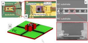 |
| Hybrid, 3D integrated optical transceiver. (A,B) The test setup: the photonic chip (PIC) is placed on a circuit board (green), and the electronic chip (EIC) is bonded on top of the photonic chip. (C) is a cross-section of the EIC-PIC assembly with �bumps. (D) Shows the mesh of the finite element model. CREDIT The Authors, doi: 10.1117/1.JOM.4.1.011004. |
Abstract:
Recent advancements in AI and more specifically large language models such as ChatGPT have put a strain on data centers. AI models require huge amounts of data to train, and in order to move data between the processing units and memory, efficient communication links become necessary. For long distance communication, fiber optics has already been the go-to solution for decades. For short distance intra-data center communication, the industry is now also starting to adopt fiber optics due to its great performance compared to classical electrical links. Recent technological developments now even enable the switch from electrical to optical interconnect for very small distances, such as the communication between chips inside the same package.
Thermal impact of 3D stacking photonic and electronic chips: Researchers investigate how the thermal penalty of 3D integration can be minimized
Bellingham, WA | Posted on December 8th, 2023This requires a conversion of the data stream from the electrical to the optical domain, which happens in the optical transceiver. Silicon photonics is the most widely used technology for fabricating these optical transceivers. The active photonic devices inside the chip (modulators and photodetectors) still require a connection with electronic drivers for powering the devices and reading the incoming data. Stacking the electronic chip (EIC) right on top of the photonic chip (PIC) by means of 3D stacking technology realizes a very tight integration of the components with low parasitic capacitance.
In research recently published in the Journal of Optical Microsystems, the thermal impact of this 3D integration is investigated. The design of the photonic chip consists of an array of ring modulators, which are known for their temperature sensitivity. In order to operate in a demanding environment, such as a data center, they need active thermal stabilization. This is implemented in the form of integrated heaters. For energy efficiency reasons, it is obvious that the power required for thermal stabilization should be minimized.
The research team from KU Leuven and imec in Belgium measured the heater efficiency of the ring modulators experimentally before and after flip-chip bonding of the EIC on the PIC. A relative loss of -43.3% in efficiency was found, which is a significant impact. Furthermore, 3D finite element simulations attributed this loss to heat spreading in the EIC. This heat spreading should be avoided, because in the ideal case all heat that is generated in the integrated heater is contained close to the photonic device. The thermal crosstalk between the photonic devices also increased by up to +44.4% after bonding the EIC, which complicates the individual thermal control.
Quantifying the thermal impact of 3D photonic-electronic integration is important, but so is the prevention of heater efficiency loss. For this reason, a thermal simulation study was conducted where typical design variables were changed with the goal of increasing the heater efficiency. It is shown that by increasing the spacing between �bumps and the photonic device, and by decreasing the interconnect linewidth, the thermal penalty of 3D integration can be minimized.
####
For more information, please click here
Contacts:
Daneet Steffens
SPIE--International Society for Optics and Photonics
Office: 360-685-5478
Copyright © SPIE--International Society for Optics and Photonics
If you have a comment, please Contact us.Issuers of news releases, not 7th Wave, Inc. or Nanotechnology Now, are solely responsible for the accuracy of the content.
Bookmark:


| Related News Press |
News and information
![]() Researchers develop molecular qubits that communicate at telecom frequencies October 3rd, 2025
Researchers develop molecular qubits that communicate at telecom frequencies October 3rd, 2025
![]() Next-generation quantum communication October 3rd, 2025
Next-generation quantum communication October 3rd, 2025
![]() "Nanoreactor" cage uses visible light for catalytic and ultra-selective cross-cycloadditions October 3rd, 2025
"Nanoreactor" cage uses visible light for catalytic and ultra-selective cross-cycloadditions October 3rd, 2025
Possible Futures
![]() Spinel-type sulfide semiconductors to operate the next-generation LEDs and solar cells For solar-cell absorbers and green-LED source October 3rd, 2025
Spinel-type sulfide semiconductors to operate the next-generation LEDs and solar cells For solar-cell absorbers and green-LED source October 3rd, 2025
Chip Technology
![]() Lab to industry: InSe wafer-scale breakthrough for future electronics August 8th, 2025
Lab to industry: InSe wafer-scale breakthrough for future electronics August 8th, 2025
![]() A 1960s idea inspires NBI researchers to study hitherto inaccessible quantum states June 6th, 2025
A 1960s idea inspires NBI researchers to study hitherto inaccessible quantum states June 6th, 2025
![]() Programmable electron-induced color router array May 14th, 2025
Programmable electron-induced color router array May 14th, 2025
Optical computing/Photonic computing
![]() ICFO researchers overcome long-standing bottleneck in single photon detection with twisted 2D materials August 8th, 2025
ICFO researchers overcome long-standing bottleneck in single photon detection with twisted 2D materials August 8th, 2025
![]() Programmable electron-induced color router array May 14th, 2025
Programmable electron-induced color router array May 14th, 2025
![]() Nanophotonic platform boosts efficiency of nonlinear-optical quantum teleportation April 25th, 2025
Nanophotonic platform boosts efficiency of nonlinear-optical quantum teleportation April 25th, 2025
![]() Groundbreaking research unveils unified theory for optical singularities in photonic microstructures December 13th, 2024
Groundbreaking research unveils unified theory for optical singularities in photonic microstructures December 13th, 2024
Discoveries
![]() Researchers develop molecular qubits that communicate at telecom frequencies October 3rd, 2025
Researchers develop molecular qubits that communicate at telecom frequencies October 3rd, 2025
![]() Next-generation quantum communication October 3rd, 2025
Next-generation quantum communication October 3rd, 2025
![]() "Nanoreactor" cage uses visible light for catalytic and ultra-selective cross-cycloadditions October 3rd, 2025
"Nanoreactor" cage uses visible light for catalytic and ultra-selective cross-cycloadditions October 3rd, 2025
Announcements
![]() Rice membrane extracts lithium from brines with greater speed, less waste October 3rd, 2025
Rice membrane extracts lithium from brines with greater speed, less waste October 3rd, 2025
![]() Researchers develop molecular qubits that communicate at telecom frequencies October 3rd, 2025
Researchers develop molecular qubits that communicate at telecom frequencies October 3rd, 2025
![]() Next-generation quantum communication October 3rd, 2025
Next-generation quantum communication October 3rd, 2025
![]() "Nanoreactor" cage uses visible light for catalytic and ultra-selective cross-cycloadditions October 3rd, 2025
"Nanoreactor" cage uses visible light for catalytic and ultra-selective cross-cycloadditions October 3rd, 2025
Interviews/Book Reviews/Essays/Reports/Podcasts/Journals/White papers/Posters
![]() Spinel-type sulfide semiconductors to operate the next-generation LEDs and solar cells For solar-cell absorbers and green-LED source October 3rd, 2025
Spinel-type sulfide semiconductors to operate the next-generation LEDs and solar cells For solar-cell absorbers and green-LED source October 3rd, 2025
![]() Rice membrane extracts lithium from brines with greater speed, less waste October 3rd, 2025
Rice membrane extracts lithium from brines with greater speed, less waste October 3rd, 2025
Photonics/Optics/Lasers
![]() ICFO researchers overcome long-standing bottleneck in single photon detection with twisted 2D materials August 8th, 2025
ICFO researchers overcome long-standing bottleneck in single photon detection with twisted 2D materials August 8th, 2025
![]() Institute for Nanoscience hosts annual proposal planning meeting May 16th, 2025
Institute for Nanoscience hosts annual proposal planning meeting May 16th, 2025
|
|
||
|
|
||
| The latest news from around the world, FREE | ||
|
|
||
|
|
||
| Premium Products | ||
|
|
||
|
Only the news you want to read!
Learn More |
||
|
|
||
|
Full-service, expert consulting
Learn More |
||
|
|
||