Home > Press > Breakthrough in the optical properties of MXenes - two-dimensional heterostructures provide new ideas
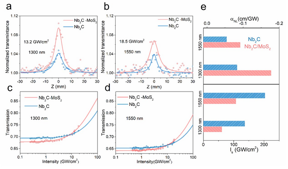 |
| OA Z-scan results of Nb2C/MoS2 and Nb2C with an excitation wavelength of (a) 1300 nm and (b) 1550 nm. The corresponding nonlinear transmittance curves under excitation optical intensity are shown in (c) and (d). (e) Fitted nonlinear optics parameter for comparison . CREDIT OEA |
Abstract:
A new publication from Opto-Electronic Advances, 10.29026/oea.2023.220162 discusses a breakthrough in the optical properties of MXenes.
Breakthrough in the optical properties of MXenes - two-dimensional heterostructures provide new ideas
Sichuan, China | Posted on May 12th, 2023Two-dimensional layered materials are a novel class of materials that exhibit strong and distinctive light-matter interactions, offering broad application prospects in optoelectronic devices and photonic elements. These materials encompass graphene, transition metal sulfides (TMDs), black phosphorus (BP), and others, which demonstrate exceptional performance characteristics such as ultrafast and wide-spectrum response, robust excitonic optical properties, and tunable direct optical band gaps.
MXenes represent a newly discovered class of two-dimensional layered materials, which showcase fascinating and tunable optical, chemical, and electronic properties, and exhibit diverse applications in fields such as photoelectricity, photothermal conversion, and photovoltaics. Furthermore, MXenes demonstrate strong nonlinear optical responses, and their nonlinear optical absorption can be adjusted by thickness, excitation wavelength, and surface groups.
In addition, the construction of two-dimensional heterostructures represents an important strategy for enhancing the optoelectronic performance of devices that utilize two-dimensional materials. By employing careful design, the advantageous properties of each component within the heterostructure can be preserved, while novel characteristics such as charge transfer or energy transfer can be generated via the interfacial effects.
The authors of this article propose a simple and effective method for preparing Nb2C/MoS2 heterostructures with enhanced both linear and nonlinear optical properties.
In this work, MoS2 nanocrystals were successfully grown on the surface of Nb2C nanosheets in situ, resulting in the construction of a two-dimensional Nb2C/MoS2 heterostructure. It was found that this heterostructure outperformed pure Nb2C in both linear and nonlinear optics.
The study reveals that the surface group of Nb2C can modulate the work function of Nb2C/MoS2, which affects the charge transfer and energy alignment between Nb2C and MoS2. As a result, Nb2C/MoS2 inherits the advantages of Nb2C and MoS2 at different wavelengths and exhibits enhanced broadband optical absorption characteristics.
Furthermore, the research demonstrates that hole transfer from Nb2C to MoS2 leads to modulation of the nonlinear optical response in the heterostructure. It also proves that Nb2C/MoS2 has stronger and tunable near-infrared nonlinear optical absorption characteristics than pure Nb2C. The nonlinear absorption coefficient of Nb2C/MoS2 is more than twice that of pure Nb2C, as illustrated in Figure 1. This study presents an effective approach for the development of broadband optoelectronic devices and optical modulators. In particular, the findings provide a strong basis for the utilization of MXenes, which exhibit excellent photoelectric performance, in the field of optoelectronics.
# # # # # #
This work was completed by the team of Hunan Key Laboratory of Nanophotonics and Devices at Central South University, led by Prof. Jun He. The team has cultivated 5 national-level young talents and 12 provincial-level talents, and independently built a photoelectron spectroscopy measurement system with femtosecond time resolution, three-dimensional spin resolution, and energy-momentum resolution.
Prof. Jun He obtained his Ph.D. from the National University of Singapore in 2006. In recognition of his achievements, he was awarded the National Outstanding Youth Science Foundation in 2012 and was selected as a Furong Scholar Distinguished Professor of Hunan Province in 2016. Currently, he focuses his research on the ultrafast phenomena and nonlinear optics of nanoscale materials, as well as the femtosecond laser fabrication of micro-nano structures and two-dimensional material neuromorphic transistor. His extensive work in this area has resulted in the publication of over 240 papers in renowned international journals such as Nature Commun. and Phys. Rev. Lett., with over 6,700 citations.
Dr. Yingwei Wang obtained his Ph.D. from Central South University in 2017. He subsequently completed postdoctoral fellow training at Shenzhen University, Jinan University, and Korea University. Currently, he serves as a lecturer in the School of Physics and Electronics at Central South University, where he focuses his research on the Nanophotonics of low-dimensional materials. In recognition of his contributions to the field, he was awarded the Outstanding Youth Science Foundation of Hunan Province in 2022.
####
About Compuscript Ltd
Opto-Electronic Advances (OEA) is a high-impact, open access, peer reviewed monthly SCI journal with an impact factor of 8.933 (Journal Citation Reports for IF2021). Since its launch in March 2018, OEA has been indexed in SCI, EI, DOAJ, Scopus, CA and ICI databases over the time and expanded its Editorial Board to 36 members from 17 countries and regions (average h-index 49).
The journal is published by The Institute of Optics and Electronics, Chinese Academy of Sciences, aiming at providing a platform for researchers, academicians, professionals, practitioners, and students to impart and share knowledge in the form of high quality empirical and theoretical research papers covering the topics of optics, photonics and optoelectronics.
For more information, please click here
Contacts:
Conor Lovett
Compuscript Ltd
Office: 353-614-75205
Copyright © Compuscript Ltd
If you have a comment, please Contact us.Issuers of news releases, not 7th Wave, Inc. or Nanotechnology Now, are solely responsible for the accuracy of the content.
Bookmark:


| Related Links |
| Related News Press |
News and information
![]() Researchers develop molecular qubits that communicate at telecom frequencies October 3rd, 2025
Researchers develop molecular qubits that communicate at telecom frequencies October 3rd, 2025
![]() Next-generation quantum communication October 3rd, 2025
Next-generation quantum communication October 3rd, 2025
![]() "Nanoreactor" cage uses visible light for catalytic and ultra-selective cross-cycloadditions October 3rd, 2025
"Nanoreactor" cage uses visible light for catalytic and ultra-selective cross-cycloadditions October 3rd, 2025
2 Dimensional Materials
![]() ICFO researchers overcome long-standing bottleneck in single photon detection with twisted 2D materials August 8th, 2025
ICFO researchers overcome long-standing bottleneck in single photon detection with twisted 2D materials August 8th, 2025
![]() First real-time observation of two-dimensional melting process: Researchers at Mainz University unveil new insights into magnetic vortex structures August 8th, 2025
First real-time observation of two-dimensional melting process: Researchers at Mainz University unveil new insights into magnetic vortex structures August 8th, 2025
![]() Lab to industry: InSe wafer-scale breakthrough for future electronics August 8th, 2025
Lab to industry: InSe wafer-scale breakthrough for future electronics August 8th, 2025
![]() Closing the gaps � MXene-coating filters can enhance performance and reusability February 28th, 2025
Closing the gaps � MXene-coating filters can enhance performance and reusability February 28th, 2025
Possible Futures
![]() Spinel-type sulfide semiconductors to operate the next-generation LEDs and solar cells For solar-cell absorbers and green-LED source October 3rd, 2025
Spinel-type sulfide semiconductors to operate the next-generation LEDs and solar cells For solar-cell absorbers and green-LED source October 3rd, 2025
Chip Technology
![]() Lab to industry: InSe wafer-scale breakthrough for future electronics August 8th, 2025
Lab to industry: InSe wafer-scale breakthrough for future electronics August 8th, 2025
![]() A 1960s idea inspires NBI researchers to study hitherto inaccessible quantum states June 6th, 2025
A 1960s idea inspires NBI researchers to study hitherto inaccessible quantum states June 6th, 2025
![]() Programmable electron-induced color router array May 14th, 2025
Programmable electron-induced color router array May 14th, 2025
Optical computing/Photonic computing
![]() ICFO researchers overcome long-standing bottleneck in single photon detection with twisted 2D materials August 8th, 2025
ICFO researchers overcome long-standing bottleneck in single photon detection with twisted 2D materials August 8th, 2025
![]() Programmable electron-induced color router array May 14th, 2025
Programmable electron-induced color router array May 14th, 2025
![]() Nanophotonic platform boosts efficiency of nonlinear-optical quantum teleportation April 25th, 2025
Nanophotonic platform boosts efficiency of nonlinear-optical quantum teleportation April 25th, 2025
![]() Groundbreaking research unveils unified theory for optical singularities in photonic microstructures December 13th, 2024
Groundbreaking research unveils unified theory for optical singularities in photonic microstructures December 13th, 2024
Discoveries
![]() Researchers develop molecular qubits that communicate at telecom frequencies October 3rd, 2025
Researchers develop molecular qubits that communicate at telecom frequencies October 3rd, 2025
![]() Next-generation quantum communication October 3rd, 2025
Next-generation quantum communication October 3rd, 2025
![]() "Nanoreactor" cage uses visible light for catalytic and ultra-selective cross-cycloadditions October 3rd, 2025
"Nanoreactor" cage uses visible light for catalytic and ultra-selective cross-cycloadditions October 3rd, 2025
Announcements
![]() Rice membrane extracts lithium from brines with greater speed, less waste October 3rd, 2025
Rice membrane extracts lithium from brines with greater speed, less waste October 3rd, 2025
![]() Researchers develop molecular qubits that communicate at telecom frequencies October 3rd, 2025
Researchers develop molecular qubits that communicate at telecom frequencies October 3rd, 2025
![]() Next-generation quantum communication October 3rd, 2025
Next-generation quantum communication October 3rd, 2025
![]() "Nanoreactor" cage uses visible light for catalytic and ultra-selective cross-cycloadditions October 3rd, 2025
"Nanoreactor" cage uses visible light for catalytic and ultra-selective cross-cycloadditions October 3rd, 2025
Interviews/Book Reviews/Essays/Reports/Podcasts/Journals/White papers/Posters
![]() Spinel-type sulfide semiconductors to operate the next-generation LEDs and solar cells For solar-cell absorbers and green-LED source October 3rd, 2025
Spinel-type sulfide semiconductors to operate the next-generation LEDs and solar cells For solar-cell absorbers and green-LED source October 3rd, 2025
![]() Rice membrane extracts lithium from brines with greater speed, less waste October 3rd, 2025
Rice membrane extracts lithium from brines with greater speed, less waste October 3rd, 2025
Photonics/Optics/Lasers
![]() ICFO researchers overcome long-standing bottleneck in single photon detection with twisted 2D materials August 8th, 2025
ICFO researchers overcome long-standing bottleneck in single photon detection with twisted 2D materials August 8th, 2025
![]() Institute for Nanoscience hosts annual proposal planning meeting May 16th, 2025
Institute for Nanoscience hosts annual proposal planning meeting May 16th, 2025
|
|
||
|
|
||
| The latest news from around the world, FREE | ||
|
|
||
|
|
||
| Premium Products | ||
|
|
||
|
Only the news you want to read!
Learn More |
||
|
|
||
|
Full-service, expert consulting
Learn More |
||
|
|
||