Home > Press > A different type of 2-D semiconductor: Berkeley Lab researchers produce first ultrathin sheets of perovskite hybrids
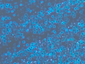 |
| Ultrathin sheets of a new 2-D hybrid perovskite are square-shaped and relatively large in area, properties that should facilitate their integration into future electronic devices. CREDIT: Courtesy of Peidong Yang, Berkeley Lab |
Abstract:
To the growing list of two-dimensional semiconductors, such as graphene, boron nitride, and molybdenum disulfide, whose unique electronic properties make them potential successors to silicon in future devices, you can now add hybrid organic-inorganic perovskites. However, unlike the other contenders, which are covalent semiconductors, these 2D hybrid perovskites are ionic materials, which gives them special properties of their own.
A different type of 2-D semiconductor: Berkeley Lab researchers produce first ultrathin sheets of perovskite hybrids
Berkeley, CA | Posted on September 26th, 2015Researchers at the U.S. Department of Energy (DOE)'s Lawrence Berkeley National Laboratory (Berkeley Lab) have successfully grown atomically thin 2D sheets of organic-inorganic hybrid perovskites from solution. The ultrathin sheets are of high quality, large in area, and square-shaped. They also exhibited efficient photoluminescence, color-tunability, and a unique structural relaxation not found in covalent semiconductor sheets.
"We believe this is the first example of 2D atomically thin nanostructures made from ionic materials," says Peidong Yang, a chemist with Berkeley Lab's Materials Sciences Division and world authority on nanostructures, who first came up with the idea for this research some 20 years ago. "The results of our study open up opportunities for fundamental research on the synthesis and characterization of atomically thin 2D hybrid perovskites and introduces a new family of 2D solution-processed semiconductors for nanoscale optoelectronic devices, such as field effect transistors and photodetectors."
Yang, who also holds appointments with the University of California (UC) Berkeley and is a co-director of the Kavli Energy NanoScience Institute (Kavli-ENSI), is the corresponding author of a paper describing this research in the journal Science. The paper is titled "Atomically thin two-dimensional organic-inorganic hybrid perovskites." The lead authors are Letian Dou, Andrew Wong and Yi Yu, all members of Yang's research group. Other authors are Minliang Lai, Nikolay Kornienko, Samuel Eaton, Anthony Fu, Connor Bischak, Jie Ma, Tina Ding, Naomi Ginsberg, Lin-Wang Wang and Paul Alivisatos.
Traditional perovskites are typically metal-oxide materials that display a wide range of fascinating electromagnetic properties, including ferroelectricity and piezoelectricity, superconductivity and colossal magnetoresistance. In the past couple of years, organic-inorganic hybrid perovskites have been solution-processed into thin films or bulk crystals for photovoltaic devices that have reached a 20-percent power conversion efficiency. Separating these hybrid materials into individual, free-standing 2D sheets through such techniques as spin-coating, chemical vapor deposition, and mechanical exfoliation has met with limited success.
In 1994, while a PhD student at Harvard University, Yang proposed a method for preparing 2D hybrid perovskite nanostructures and tuning their electronic properties but never acted upon it. This past year, while preparing to move his office, he came upon the proposal and passed it on to co-lead author Dou, a post-doctoral student in his research group. Dou, working mainly with the other lead authors Wong and Yu, used Yang's proposal to synthesize free-standing 2D sheets of CH3NH3PbI3, a hybrid perovskite made from a blend of lead, bromine, nitrogen, carbon and hydrogen atoms.
"Unlike exfoliation and chemical vapor deposition methods, which normally produce relatively thick perovskite plates, we were able to grow uniform square-shaped 2D crystals on a flat substrate with high yield and excellent reproducibility," says Dou. "We characterized the structure and composition of individual 2D crystals using a variety of techniques and found they have a slightly shifted band-edge emission that could be attributed to structural relaxation. A preliminary photoluminescence study indicates a band-edge emission at 453 nanometers, which is red-shifted slightly as compared to bulk crystals. This suggests that color-tuning could be achieved in these 2D hybrid perovskites by changing sheet thickness as well as composition via the synthesis of related materials."
The well-defined geometry of these square-shaped 2D crystals is the mark of high quality crystallinity, and their large size should facilitate their integration into future devices.
"With our technique, vertical and lateral heterostructures can also be achieved," Yang says. "This opens up new possibilities for the design of materials/devices on an atomic/molecular scale with distinctive new properties."
###
This research was supported by DOE's Office of Science. The characterization work was carried out at the Molecular Foundry's National Center for Electron Microscopy, and at beamline 7.3.3 of the Advanced Light Source. Both the Molecular Foundry and the Advanced Light Source are DOE Office of Science User Facilities hosted at Berkeley Lab.
####
About DOE/Lawrence Berkeley National Laboratory
Lawrence Berkeley National Laboratory addresses the world's most urgent scientific challenges by advancing sustainable energy, protecting human health, creating new materials, and revealing the origin and fate of the universe. Founded in 1931, Berkeley Lab's scientific expertise has been recognized with 13 Nobel prizes. The University of California manages Berkeley Lab for the U.S. Department of Energy's Office of Science. For more, visit www.lbl.gov.
DOE's Office of Science is the single largest supporter of basic research in the physical sciences in the United States, and is working to address some of the most pressing challenges of our time. For more information, please visit the Office of Science website at science.energy.gov/.
For more information, please click here
Contacts:
Lynn Yarris
510-486-5375
Copyright © DOE/Lawrence Berkeley National Laboratory
If you have a comment, please Contact us.Issuers of news releases, not 7th Wave, Inc. or Nanotechnology Now, are solely responsible for the accuracy of the content.
Bookmark:


| Related News Press |
News and information
![]() Quantum computer improves AI predictions April 17th, 2026
Quantum computer improves AI predictions April 17th, 2026
![]() Flexible sensor gains sensitivity under pressure April 17th, 2026
Flexible sensor gains sensitivity under pressure April 17th, 2026
![]() A reusable chip for particulate matter sensing April 17th, 2026
A reusable chip for particulate matter sensing April 17th, 2026
![]() Detecting vibrational quantum beating in the predissociation dynamics of SF6 using time-resolved photoelectron spectroscopy April 17th, 2026
Detecting vibrational quantum beating in the predissociation dynamics of SF6 using time-resolved photoelectron spectroscopy April 17th, 2026
Laboratories
![]() Researchers develop molecular qubits that communicate at telecom frequencies October 3rd, 2025
Researchers develop molecular qubits that communicate at telecom frequencies October 3rd, 2025
![]() A battery�s hopping ions remember where they�ve been: Seen in atomic detail, the seemingly smooth flow of ions through a battery�s electrolyte is surprisingly complicated February 16th, 2024
A battery�s hopping ions remember where they�ve been: Seen in atomic detail, the seemingly smooth flow of ions through a battery�s electrolyte is surprisingly complicated February 16th, 2024
Govt.-Legislation/Regulation/Funding/Policy
![]() Quantum computer improves AI predictions April 17th, 2026
Quantum computer improves AI predictions April 17th, 2026
![]() Metasurfaces smooth light to boost magnetic sensing precision January 30th, 2026
Metasurfaces smooth light to boost magnetic sensing precision January 30th, 2026
![]() New imaging approach transforms study of bacterial biofilms August 8th, 2025
New imaging approach transforms study of bacterial biofilms August 8th, 2025
Possible Futures
![]() A fundamentally new therapeutic approach to cystic fibrosis: Nanobody repairs cellular defect April 17th, 2026
A fundamentally new therapeutic approach to cystic fibrosis: Nanobody repairs cellular defect April 17th, 2026
![]() UC Irvine physicists discover method to reverse �quantum scrambling� : The work addresses the problem of information loss in quantum computing system April 17th, 2026
UC Irvine physicists discover method to reverse �quantum scrambling� : The work addresses the problem of information loss in quantum computing system April 17th, 2026
Molecular Nanotechnology
![]() Quantum pumping in molecular junctions August 16th, 2024
Quantum pumping in molecular junctions August 16th, 2024
![]() Scientists push the boundaries of manipulating light at the submicroscopic level March 3rd, 2023
Scientists push the boundaries of manipulating light at the submicroscopic level March 3rd, 2023
![]() First electric nanomotor made from DNA material: Synthetic rotary motors at the nanoscale perform mechanical work July 22nd, 2022
First electric nanomotor made from DNA material: Synthetic rotary motors at the nanoscale perform mechanical work July 22nd, 2022
Discoveries
![]() Quantum computer improves AI predictions April 17th, 2026
Quantum computer improves AI predictions April 17th, 2026
![]() Flexible sensor gains sensitivity under pressure April 17th, 2026
Flexible sensor gains sensitivity under pressure April 17th, 2026
![]() A reusable chip for particulate matter sensing April 17th, 2026
A reusable chip for particulate matter sensing April 17th, 2026
![]() Detecting vibrational quantum beating in the predissociation dynamics of SF6 using time-resolved photoelectron spectroscopy April 17th, 2026
Detecting vibrational quantum beating in the predissociation dynamics of SF6 using time-resolved photoelectron spectroscopy April 17th, 2026
Materials/Metamaterials/Magnetoresistance
![]() First real-time observation of two-dimensional melting process: Researchers at Mainz University unveil new insights into magnetic vortex structures August 8th, 2025
First real-time observation of two-dimensional melting process: Researchers at Mainz University unveil new insights into magnetic vortex structures August 8th, 2025
![]() Researchers unveil a groundbreaking clay-based solution to capture carbon dioxide and combat climate change June 6th, 2025
Researchers unveil a groundbreaking clay-based solution to capture carbon dioxide and combat climate change June 6th, 2025
![]() A 1960s idea inspires NBI researchers to study hitherto inaccessible quantum states June 6th, 2025
A 1960s idea inspires NBI researchers to study hitherto inaccessible quantum states June 6th, 2025
![]() Institute for Nanoscience hosts annual proposal planning meeting May 16th, 2025
Institute for Nanoscience hosts annual proposal planning meeting May 16th, 2025
Announcements
![]() A fundamentally new therapeutic approach to cystic fibrosis: Nanobody repairs cellular defect April 17th, 2026
A fundamentally new therapeutic approach to cystic fibrosis: Nanobody repairs cellular defect April 17th, 2026
![]() UC Irvine physicists discover method to reverse �quantum scrambling� : The work addresses the problem of information loss in quantum computing system April 17th, 2026
UC Irvine physicists discover method to reverse �quantum scrambling� : The work addresses the problem of information loss in quantum computing system April 17th, 2026
Interviews/Book Reviews/Essays/Reports/Podcasts/Journals/White papers/Posters
![]() A fundamentally new therapeutic approach to cystic fibrosis: Nanobody repairs cellular defect April 17th, 2026
A fundamentally new therapeutic approach to cystic fibrosis: Nanobody repairs cellular defect April 17th, 2026
![]() UC Irvine physicists discover method to reverse �quantum scrambling� : The work addresses the problem of information loss in quantum computing system April 17th, 2026
UC Irvine physicists discover method to reverse �quantum scrambling� : The work addresses the problem of information loss in quantum computing system April 17th, 2026
Energy
![]() Sensors innovations for smart lithium-based batteries: advancements, opportunities, and potential challenges August 8th, 2025
Sensors innovations for smart lithium-based batteries: advancements, opportunities, and potential challenges August 8th, 2025
![]() Simple algorithm paired with standard imaging tool could predict failure in lithium metal batteries August 8th, 2025
Simple algorithm paired with standard imaging tool could predict failure in lithium metal batteries August 8th, 2025
Solar/Photovoltaic
![]() Spinel-type sulfide semiconductors to operate the next-generation LEDs and solar cells For solar-cell absorbers and green-LED source October 3rd, 2025
Spinel-type sulfide semiconductors to operate the next-generation LEDs and solar cells For solar-cell absorbers and green-LED source October 3rd, 2025
![]() KAIST researchers introduce new and improved, next-generation perovskite solar cell November 8th, 2024
KAIST researchers introduce new and improved, next-generation perovskite solar cell November 8th, 2024
![]() Groundbreaking precision in single-molecule optoelectronics August 16th, 2024
Groundbreaking precision in single-molecule optoelectronics August 16th, 2024
![]() Development of zinc oxide nanopagoda array photoelectrode: photoelectrochemical water-splitting hydrogen production January 12th, 2024
Development of zinc oxide nanopagoda array photoelectrode: photoelectrochemical water-splitting hydrogen production January 12th, 2024
|
|
||
|
|
||
| The latest news from around the world, FREE | ||
|
|
||
|
|
||
| Premium Products | ||
|
|
||
|
Only the news you want to read!
Learn More |
||
|
|
||
|
Full-service, expert consulting
Learn More |
||
|
|
||