Home > Press > Non-Destructive Hall Mobility Testing for Semiconductor, Solar offered by Lehighton Electronics’ New LEI 1605
 |
Abstract:
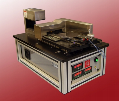
Lehighton Electronics, Inc (LEI) announces the introduction of its new LEI 1605 Mobility Tester for semiconductor and solar manufacturing processes. The LEI 1605 manually measures electron mobility (EM) through a non-destructive contactless means on a variety of substrates and materials.
Non-Destructive Hall Mobility Testing for Semiconductor, Solar offered by Lehighton Electronics’ New LEI 1605
Lehighton, PA | Posted on February 27th, 2009The LEI 1605 is ideal for process development, prototyping, low-volume and small batch production. It is the newest product in Lehighton's line of mobility equipment geared toward universities and R&D centers. Its manual operation and thus lower cost make it an attractive and practical research alternative to the automatic, more expensive solutions that LEI offers for production volumes.
The LEI 1605 replaces the destructive van der Pauw Hall and Parallelepiped or Bridge Type methods currently used to achieve electron mobility, carrier density, carrier concentration and sheet resistance measures. The LEI 1605 provides critical, accurate process control measurements in situ. With the LEI 1605, researchers can measure electron mobility after each epitaxial layer deposition, enhancing their ability to monitor specific stages of process control. The LEI 1605 with optional upgrades will measure electron mobility in the range of ~300-20,000 cm2/v.sec, and will measure sheet resistance from ~100Ω-3kΩ/square and possesses mapping capability.
The LEI 1605 reduces the cost of research by providing EM results instantly, allowing operators to make changes for optimal processing. The destructive Hall tests do not allow substrates to be recycled and reused; the LEI1605 eliminates this waste by allowing the reuse of wafers repeatedly. With this tool, there is no more cleaving, soldering and hoping for good connections and test results. This ultimately leads to more research of more concepts due to quick results, low risk factors, and low cost consumption. More research in shorter time with in-situ testing can lead to more projects and more funding.
####
About Lehighton Electronics, Inc
Lehighton Electronics Inc. has been engineering and providing metrology solutions to the silicon, compound semiconductor, solar, flat panel display and other related industries for more than 40 years. Some tools sold in the 1970s are still used in production today, providing our customers with consistently low tool ownership and operating costs.
For more information, please click here
Contacts:
Robert Warren
(800) 535-1112
Phone: 610-377-5990
Fax: 610-377-6820
Copyright © Lehighton Electronics, Inc
If you have a comment, please Contact us.Issuers of news releases, not 7th Wave, Inc. or Nanotechnology Now, are solely responsible for the accuracy of the content.
Bookmark:


| Related News Press |
News and information
![]() Quantum computer improves AI predictions April 17th, 2026
Quantum computer improves AI predictions April 17th, 2026
![]() Flexible sensor gains sensitivity under pressure April 17th, 2026
Flexible sensor gains sensitivity under pressure April 17th, 2026
![]() A reusable chip for particulate matter sensing April 17th, 2026
A reusable chip for particulate matter sensing April 17th, 2026
![]() Detecting vibrational quantum beating in the predissociation dynamics of SF6 using time-resolved photoelectron spectroscopy April 17th, 2026
Detecting vibrational quantum beating in the predissociation dynamics of SF6 using time-resolved photoelectron spectroscopy April 17th, 2026
Chip Technology
![]() A reusable chip for particulate matter sensing April 17th, 2026
A reusable chip for particulate matter sensing April 17th, 2026
![]() Metasurfaces smooth light to boost magnetic sensing precision January 30th, 2026
Metasurfaces smooth light to boost magnetic sensing precision January 30th, 2026
Announcements
![]() A fundamentally new therapeutic approach to cystic fibrosis: Nanobody repairs cellular defect April 17th, 2026
A fundamentally new therapeutic approach to cystic fibrosis: Nanobody repairs cellular defect April 17th, 2026
![]() UC Irvine physicists discover method to reverse ‘quantum scrambling’ : The work addresses the problem of information loss in quantum computing system April 17th, 2026
UC Irvine physicists discover method to reverse ‘quantum scrambling’ : The work addresses the problem of information loss in quantum computing system April 17th, 2026
Tools
![]() Metasurfaces smooth light to boost magnetic sensing precision January 30th, 2026
Metasurfaces smooth light to boost magnetic sensing precision January 30th, 2026
![]() From sensors to smart systems: the rise of AI-driven photonic noses January 30th, 2026
From sensors to smart systems: the rise of AI-driven photonic noses January 30th, 2026
![]() Japan launches fully domestically produced quantum computer: Expo visitors to experience quantum computing firsthand August 8th, 2025
Japan launches fully domestically produced quantum computer: Expo visitors to experience quantum computing firsthand August 8th, 2025
|
|
||
|
|
||
| The latest news from around the world, FREE | ||
|
|
||
|
|
||
| Premium Products | ||
|
|
||
|
Only the news you want to read!
Learn More |
||
|
|
||
|
Full-service, expert consulting
Learn More |
||
|
|
||