Home > Press > Writing between the lines: Nano-patterning on silicon: a single compound reacts with silicon surface to form perpendicular molecular lines
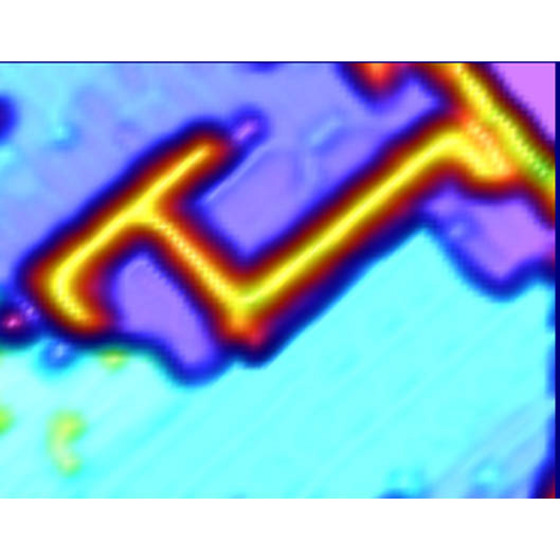 |
| Figure 1: Scanning-tunneling microscopy image of acetophenone lines on a silicon surface. The lines of acetophenone can be seen as a bright orange line against the blue background of the surface. |
Abstract:
Miniaturization of microprocessor components can be achieved by two opposing methods: so-called top-down and bottom-up approaches. In top-down approaches, smaller and smaller circuits are produced by optimizing and improving upon larger scale patterning technology. Bottom-up approaches rely on the assembly of single molecule building blocks to produce patterns—ultimately, the pattern size that can be achieved by either method will coincide. One potential bottom-up method creates molecular lines—and ultimately patterns—by reacting molecules with the atoms at the surface of a material. The major challenge for researchers is to control the direction in which these lines grow.
Writing between the lines: Nano-patterning on silicon: a single compound reacts with silicon surface to form perpendicular molecular lines
Japan | Posted on December 26th, 2008Most microprocessor devices are produced from silicon, so patterning of silicon surfaces is of high importance. Writing in the Journal of the American Chemical Society1, Md. Zakir Hossain and co-workers from the RIKEN Advanced Science Institute in Wako have shown that reaction of a single compound—acetophenone—with a silicon surface can result in the growth of straight lines of molecules (Fig. 1).
The surface of the silicon comprises pairs of silicon atoms, known as dimers, arranged in parallel rows. Various molecules have been previously shown to form straight lines by reaction with the surface of the silicon—either along the dimer rows or perpendicular to them. Importantly, the direction of growth of these lines depended—until now—only on the molecule reacting with the silicon surface.
The silicon surface is prepared by reaction with atomic hydrogen, which results in silicon hydrogen bonds over most of the surface. However a few silicon atoms do not react, forming so called dangling bond sites, which are very reactive. Acetophenone molecules react with the dangling bond and go on to create a new dangling bond site at an adjacent silicon dimer. This sets up a chain reaction and produces a molecular line. The direction in which the lines of molecules grow depends on whether the new dangling bond is formed in a silicon dimer in the same row or a parallel row.
The distance between silicon dimers in the same row or those in adjacent rows is different, and there is a consequent energy difference in the two possible growth directions. "Acetophenone happens to have a geometry that means it can grow lines in either direction," explains Hossain. "Creation of a chiral center upon adsorption also seems to play important role in producing lines in both directions, which we believe will provide opportunities to control the growth direction."
Reference
1. Hossain, M. Z., Kato, H. S. & Kawai, M. Self-directed chain reaction by small ketones with the dangling bond site on the Si(100)-(2 x 1)-H surface: acetophenone, a unique example. Journal of the American Chemical Society 130, 11518-11523 (2008).
The corresponding author for this highlight is based at the RIKEN Surface Chemistry Laboratory
####
For more information, please click here
Copyright © Riken
If you have a comment, please Contact us.Issuers of news releases, not 7th Wave, Inc. or Nanotechnology Now, are solely responsible for the accuracy of the content.
Bookmark:


| Related Links |
| Related News Press |
News and information
![]() Quantum computer improves AI predictions April 17th, 2026
Quantum computer improves AI predictions April 17th, 2026
![]() Flexible sensor gains sensitivity under pressure April 17th, 2026
Flexible sensor gains sensitivity under pressure April 17th, 2026
![]() A reusable chip for particulate matter sensing April 17th, 2026
A reusable chip for particulate matter sensing April 17th, 2026
![]() Detecting vibrational quantum beating in the predissociation dynamics of SF6 using time-resolved photoelectron spectroscopy April 17th, 2026
Detecting vibrational quantum beating in the predissociation dynamics of SF6 using time-resolved photoelectron spectroscopy April 17th, 2026
Chip Technology
![]() A reusable chip for particulate matter sensing April 17th, 2026
A reusable chip for particulate matter sensing April 17th, 2026
![]() Metasurfaces smooth light to boost magnetic sensing precision January 30th, 2026
Metasurfaces smooth light to boost magnetic sensing precision January 30th, 2026
Discoveries
![]() Quantum computer improves AI predictions April 17th, 2026
Quantum computer improves AI predictions April 17th, 2026
![]() Flexible sensor gains sensitivity under pressure April 17th, 2026
Flexible sensor gains sensitivity under pressure April 17th, 2026
![]() A reusable chip for particulate matter sensing April 17th, 2026
A reusable chip for particulate matter sensing April 17th, 2026
![]() Detecting vibrational quantum beating in the predissociation dynamics of SF6 using time-resolved photoelectron spectroscopy April 17th, 2026
Detecting vibrational quantum beating in the predissociation dynamics of SF6 using time-resolved photoelectron spectroscopy April 17th, 2026
Announcements
![]() A fundamentally new therapeutic approach to cystic fibrosis: Nanobody repairs cellular defect April 17th, 2026
A fundamentally new therapeutic approach to cystic fibrosis: Nanobody repairs cellular defect April 17th, 2026
![]() UC Irvine physicists discover method to reverse ‘quantum scrambling’ : The work addresses the problem of information loss in quantum computing system April 17th, 2026
UC Irvine physicists discover method to reverse ‘quantum scrambling’ : The work addresses the problem of information loss in quantum computing system April 17th, 2026
|
|
||
|
|
||
| The latest news from around the world, FREE | ||
|
|
||
|
|
||
| Premium Products | ||
|
|
||
|
Only the news you want to read!
Learn More |
||
|
|
||
|
Full-service, expert consulting
Learn More |
||
|
|
||