Home > Press > Cracking a Tough Nut for the Semiconductor Industry
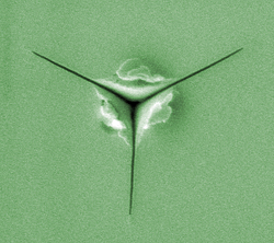 |
| Typical low-k film test for material toughness using the new NIST technique. The indentation instrument that punches the triangular hole registers the forces involved. That plus the length of the resulting cracks determines the toughness of the film, which is about 2.4 micrometers thick. (Color added for clarity.)
Credit: NIST |
Abstract:
Researchers at the National Institute of Standards and Technology (NIST) have developed a method to measure the toughness—the resistance to fracture—of the thin insulating films that play a critical role in high-performance integrated circuits. The new technique could help improve the reliability and manufacturability of ICs and, better yet, it's one that state-of-the-art microelectronics manufacturers can use with equipment they already own.
Cracking a Tough Nut for the Semiconductor Industry
GAITHERSBURG, MD | Posted on December 23rd, 2008At issue is the mechanical strength of so-called "low-k" dielectric layers—electrically insulating films only a couple of micrometers thick that are interleaved between layers of conductors and components in microprocessor chips and other high-performance semiconductor devices. As IC features like transistors have gotten ever smaller and crammed more closely together, designers are preventing electrical interference or "cross-talk" by making the insulating films more and more porous with nanoscale voids—but this has made them more fragile. Brittle fracture failure of low-k insulating films remains a problem for the industry, affecting both manufacturing yields and device reliability. To date, there has been no accurate method to measure the fracture resistance of such films, which makes it difficult to design improved dielectrics.
NIST researchers believe they have found an answer to the measurement problem in a new adaptation of a materials test technique called nanoindentation. Nanoindentation works by pressing a sharp, hard object—a diamond tip—and observing how much pressure it takes to deform the material. For roughly 20 years, researchers have known how to measure elasticity and plasticity—the forces needed to bend a material either temporarily or permanently—of materials at very small scales with nanoindenters. But toughness, the force needed to actually break the material, has been, well, tougher. Thin films were particularly problematic because they necessarily must be layered on top of another stronger material, such as a silicon wafer.
The new NIST technique requires a slight modification of the nanoindentation equipment—the probe has to have a sharper, more acute point than normally used—and a hefty dose of theory. Pressing carefully on the dielectric film generates cracks as small as 300 nanometers, which are measured by electron microscopy. Just how the cracks form depends on a complex interaction involving indentation force, film thickness, film stress and the elastic properties of the film and the silicon substrate. These variables are plugged into a new fracture mechanics model that predicts not only the fracture toughness but also another key value, the critical film thickness for spontaneous fracture.
Using this methodology, device manufacturers will be able to eliminate some candidate interconnect dielectric films from consideration without further expensive device testing. The measurement technique and model were published in a two-part series in the Journal of Materials Research.*
* D.J. Morris and R.F. Cook. Indentation fracture of low-dielectric constant films: Part I. Experiments and observations. J. Mater. Res., Vol. 23, No. 9, p. 2429.
* D.J. Morris and R.F. Cook. Indentation fracture of low-dielectric constant films: Part II. Indentation fracture mechanics model. J. Mater. Res., Vol. 23, No. 9, p. 2443.
####
About NIST
Founded in 1901, NIST is a non-regulatory federal agency within the U.S. Department of Commerce. NIST's mission is to promote U.S. innovation and industrial competitiveness by advancing measurement science, standards, and technology in ways that enhance economic security and improve our quality of life.
For more information, please click here
Contacts:
Michael Baum
(301) 975-2763
Copyright © NIST
If you have a comment, please Contact us.Issuers of news releases, not 7th Wave, Inc. or Nanotechnology Now, are solely responsible for the accuracy of the content.
Bookmark:


| Related News Press |
News and information
![]() Quantum computer improves AI predictions April 17th, 2026
Quantum computer improves AI predictions April 17th, 2026
![]() Flexible sensor gains sensitivity under pressure April 17th, 2026
Flexible sensor gains sensitivity under pressure April 17th, 2026
![]() A reusable chip for particulate matter sensing April 17th, 2026
A reusable chip for particulate matter sensing April 17th, 2026
![]() Detecting vibrational quantum beating in the predissociation dynamics of SF6 using time-resolved photoelectron spectroscopy April 17th, 2026
Detecting vibrational quantum beating in the predissociation dynamics of SF6 using time-resolved photoelectron spectroscopy April 17th, 2026
Chip Technology
![]() A reusable chip for particulate matter sensing April 17th, 2026
A reusable chip for particulate matter sensing April 17th, 2026
![]() Metasurfaces smooth light to boost magnetic sensing precision January 30th, 2026
Metasurfaces smooth light to boost magnetic sensing precision January 30th, 2026
Discoveries
![]() Quantum computer improves AI predictions April 17th, 2026
Quantum computer improves AI predictions April 17th, 2026
![]() Flexible sensor gains sensitivity under pressure April 17th, 2026
Flexible sensor gains sensitivity under pressure April 17th, 2026
![]() A reusable chip for particulate matter sensing April 17th, 2026
A reusable chip for particulate matter sensing April 17th, 2026
![]() Detecting vibrational quantum beating in the predissociation dynamics of SF6 using time-resolved photoelectron spectroscopy April 17th, 2026
Detecting vibrational quantum beating in the predissociation dynamics of SF6 using time-resolved photoelectron spectroscopy April 17th, 2026
Announcements
![]() A fundamentally new therapeutic approach to cystic fibrosis: Nanobody repairs cellular defect April 17th, 2026
A fundamentally new therapeutic approach to cystic fibrosis: Nanobody repairs cellular defect April 17th, 2026
![]() UC Irvine physicists discover method to reverse ‘quantum scrambling’ : The work addresses the problem of information loss in quantum computing system April 17th, 2026
UC Irvine physicists discover method to reverse ‘quantum scrambling’ : The work addresses the problem of information loss in quantum computing system April 17th, 2026
|
|
||
|
|
||
| The latest news from around the world, FREE | ||
|
|
||
|
|
||
| Premium Products | ||
|
|
||
|
Only the news you want to read!
Learn More |
||
|
|
||
|
Full-service, expert consulting
Learn More |
||
|
|
||