Home > Press > A new solution to graphene production
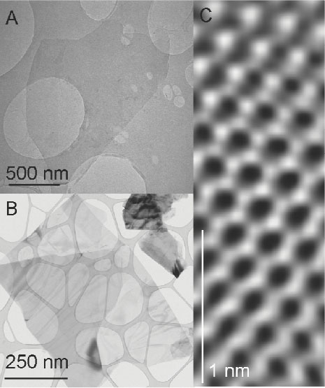 |
| Figure 1. A transmission electron microscope image of (A) a graphene monolayer and (B) a folded graphene monolayer. (C) An atomic resolution image of a portion of a graphene monolayer. (Courtesy of Valeria Nicolosi.) |
Abstract:
A liquid phase process for making defect-free graphene in high yield could pave the way for superfast transistors.
A new solution to graphene production
Bellingham, WA | Posted on November 24th, 2008As every schoolboy knows, the stuff in your pencil lead is graphite, a naturally occurring form of carbon, useful but not very interesting. What is more interesting is that graphite is made from a stacked system of layers, each just one atom thick. It was long thought that these graphene layers were unstable and that removing them from the parent crystal would cause them to roll up. This raised the question of how thin you could make graphite. Ten layers? Five? By peeling layers from a graphite crystal with sticky tape and then rubbing them onto a silicon dioxide surface, a team from the University of Manchester found a surprising answer: it is possible to produce graphite crystals just one atom thick.1 It soon became clear that this graphene had intriguing electronic properties. For example, due to the symmetry of its 2D honeycomb lattice, charge carriers in graphene appear massless.2 More important for microelectronic engineers, these carriers have ultrahigh mobility, opening the door to superfast transistors.3
The huge potential of graphene comes with one small catch: mechanical cleavage of graphite is a very slow process with very low throughput. As a result, graphene is the most expensive material known to man, costing approximately $1 per square micron.4 New, high-yield, cheap ways to make graphene are urgently needed. For microelectronics, the solution will probably be to grow graphene on silicon wafers using reasonably well known processes. However, for most other applications it is accepted that a method to produce graphene in liquids is required. Much progress has been made, with a number of groups having developed chemical techniques to split graphite into sheets of graphene-like material such as graphene oxide.5, 6 However, such materials tend to have many defects, thus altering the interesting properties. Attempting to resolve this problem, we recently demonstrated an alternative liquid-based process to exfoliate graphite to give defect-free graphene.7
We used methods developed recently to obtain individual carbon nanotubes suspended in liquids. Nanotubes tend to aggregate together, which reduces their energy. But you can remove this propensity to aggregate if you place them in a liquid that binds to the nanotubes as well as they bind to each other. We found that liquids whose surface energy matched that of nanotubes gave stable suspensions of individual nanotubes.8 As nanotubes are rolled-up graphene, we suspected the same approach would allow us to split graphite into graphene.
We mixed graphite with a nanotube-suspending solvent and applied sonic energy. Initial tests showed that significant quantities of graphite could be suspended in this manner. To test whether the science was the same as for nanotube suspensions, we mixed graphite with dozens of carefully chosen solvents and measured how much graphite remained suspended after centrifugation. When plotted versus surface energy, it became clear that the amount of suspended graphite peaked sharply for solvents with surface energy close to that expected for graphite. The mechanism was the same.
The key question was, Had we suspended graphene or just small flakes of graphite? The high boiling point of our solvents precluded the standard approach of depositing the flakes on a surface and examining with a microscope. Instead of this, we dropped the suspension on special holey substrates designed for electron microscopy. The solvent tended to run off the substrates leaving small flakes deposited in its wake that could easily be found using a transmission electron microscope. We used electron diffraction to confirm the presence of monolayers and to estimate the number of layers by focusing on the flake edges. It was immediately apparent that about 30% of them were one atomic layer thick, similar to the monolayer shown in Figure 1(A). In addition, a number of bilayers, multilayers, and folded monolayers, as shown in Figure 1(B), were observed.
To make real progress, however, we had to show that the graphene was chemically unmodified and not highly defective. As a test, we used x-ray photoelectron spectroscopy, a technique that gives information on bonding in a material. This clearly showed that the graphene was not chemically modified. But the results did not rule out the possibility of defects. Consequently, we carried out Raman spectroscopy with the help of collaborators at the University of Cambridge. With great care, Raman spectra were obtained from individual graphene flakes, giving information on the presence of defects. The answer was unambiguous. The level was too low to measure, showing that our liquid processing was not introducing defects. The high quality of the graphene was elegantly confirmed by atomic resolution transmission electron microscopy, carried out by colleagues at the University of Oxford: see Figure 1(C). In principle, this production process can be scaled up to make very large quantities of defect-free graphene.
For now, it is becoming clear that graphene can be produced, cheaply and easily, in certain liquids at a reasonable yield. In the future, we hope to improve the yield, increase the flake size, and extend this method to aqueous systems. We expect that this method will be useful, not only as a low-cost and straightforward way to make graphene, but as an enabling technology for applications such as graphene-based composites and coatings.
We acknowledge financial support from Science Foundation Ireland.
Jonathan Coleman
School of Physics and
Centre for Adaptive Nanostructures and Nanodevices (CRANN)
Trinity College Dublin
Dublin, Ireland
Jonathan Coleman is an associate professor in the School of Physics and a principal investigator at CRANN. His current research focuses on the dispersion and exfoliation of nanomaterials. He also works on the production of functional nanostructured materials such as composites and thin films for electrical and mechanical applications.
References:
1. K. S. Novoselov, A. K. Geim, S. V. Morozov, D. Jiang, Y. Zhang, S. V. Dubonos, I. V. Grigorieva, A. A. Firsov, Electric field effect in atomically thin carbon films, Science 306, no. 5696, pp. 666-669, 2004.
2. K. S. Novoselov, A. K. Geim, S. V. Morozov, D. Jiang, M. I. Katsnelson, I. V. Grigorieva, S. V. Dubonos, A. A. Firsov, Two-dimensional gas of massless Dirac fermions in graphene, Nature 438, no. 7065, pp. 197-200, 2005.
3. S. V. Morozov, K. S. Novoselov, M. I. Katsnelson, F. Schedin, D. C. Elias, J. A. Jaszczak, A. K. Geim, Giant intrinsic carrier mobilities in graphene and its bilayer, Phys. Rev. Lett. 1, no. 1, pp. 016602, 2008.
4. http://www.grapheneindustries.com/ Homepage of a commercial supplier of graphenes. Accessed 9 October 2008.
5. G. Eda, G. Fanchini, M. Chhowalla, Large-area ultrathin films of reduced graphene oxide as a transparent and flexible electronic material, Nat. Nanotechnol. 3, pp. 270-274, 2008.
6. S. Stankovich, D. A. Dikin, R. D. Piner, K. A. Kohlhaas, A. Kleinhammes, Y. Jia, Y. Wu, S. T. Nguyen, R. S. Ruoff, Synthesis of graphene-based nanosheets via chemical reduction of exfoliated graphite oxide, Carbon 45, no. 7, pp. 1558-1565, 2007.
7. Y. Hernandez, V. Nicolosi, M. Lotya, F. M. Blighe, Z. Sun, S. De, I. T. McGovern, B. Holland, M. Byrne, Y. K. Gun'ko, J. J. Boland, P. Niraj, G. Duesberg, S. Krishnamurthy, R. Goodhue, J. Hutchison, V. Scardaci, A. C. Ferrari, J. N. Coleman, High-yield production of graphene by liquid-phase exfoliation of graphite, Nat. Nanotechnol. 3, no. 9, pp. 563-568, 2008.
8. S. D. Bergin, V. Nicolosi, P. V. Streich, S. Giordani, Z. Sun, A. H. Windle, P. Ryan, N. P. P. Niraj, Z. T. Wang, L. Carpenter, W. J. Blau, J. J. Boland, J. P. Hamilton, J. N. Coleman, Towards solutions of SWNT in common solvents, Adv. Mater. 20, no. 10, pp. 1876-1881, 2007.
DOI: 10.1117/2.1200810.1336
####
About SPIE
SPIE is an international membership society, serving scientists and engineers in industry, academia, and government, as well as companies producing leading-edge products. SPIE constituents work in a wide variety of fields that utilize some aspect of optics and photonics, which is the science and application of light. More specifically, optics is a branch of physics that examines the behavior and properties of light and the interaction of light with matter. Photonics is the science and technology of generating, controlling, and detecting photons, which are particles of light.
For more information, please click here
Contacts:
SPIE
1000 20th St.
Bellingham WA 98225-6705 USA
Phone: +1 360 676 3290
or +1 888 504 8171
FAX: +1 360 647 1445
Copyright © SPIE
If you have a comment, please Contact us.Issuers of news releases, not 7th Wave, Inc. or Nanotechnology Now, are solely responsible for the accuracy of the content.
Bookmark:


| Related News Press |
News and information
![]() Quantum computer improves AI predictions April 17th, 2026
Quantum computer improves AI predictions April 17th, 2026
![]() Flexible sensor gains sensitivity under pressure April 17th, 2026
Flexible sensor gains sensitivity under pressure April 17th, 2026
![]() A reusable chip for particulate matter sensing April 17th, 2026
A reusable chip for particulate matter sensing April 17th, 2026
![]() Detecting vibrational quantum beating in the predissociation dynamics of SF6 using time-resolved photoelectron spectroscopy April 17th, 2026
Detecting vibrational quantum beating in the predissociation dynamics of SF6 using time-resolved photoelectron spectroscopy April 17th, 2026
Chip Technology
![]() A reusable chip for particulate matter sensing April 17th, 2026
A reusable chip for particulate matter sensing April 17th, 2026
![]() Metasurfaces smooth light to boost magnetic sensing precision January 30th, 2026
Metasurfaces smooth light to boost magnetic sensing precision January 30th, 2026
Discoveries
![]() Quantum computer improves AI predictions April 17th, 2026
Quantum computer improves AI predictions April 17th, 2026
![]() Flexible sensor gains sensitivity under pressure April 17th, 2026
Flexible sensor gains sensitivity under pressure April 17th, 2026
![]() A reusable chip for particulate matter sensing April 17th, 2026
A reusable chip for particulate matter sensing April 17th, 2026
![]() Detecting vibrational quantum beating in the predissociation dynamics of SF6 using time-resolved photoelectron spectroscopy April 17th, 2026
Detecting vibrational quantum beating in the predissociation dynamics of SF6 using time-resolved photoelectron spectroscopy April 17th, 2026
Announcements
![]() A fundamentally new therapeutic approach to cystic fibrosis: Nanobody repairs cellular defect April 17th, 2026
A fundamentally new therapeutic approach to cystic fibrosis: Nanobody repairs cellular defect April 17th, 2026
![]() UC Irvine physicists discover method to reverse �quantum scrambling� : The work addresses the problem of information loss in quantum computing system April 17th, 2026
UC Irvine physicists discover method to reverse �quantum scrambling� : The work addresses the problem of information loss in quantum computing system April 17th, 2026
|
|
||
|
|
||
| The latest news from around the world, FREE | ||
|
|
||
|
|
||
| Premium Products | ||
|
|
||
|
Only the news you want to read!
Learn More |
||
|
|
||
|
Full-service, expert consulting
Learn More |
||
|
|
||