Home > Press > LayTec to develop in-situ sensor for ISE’s triple-junction PV cells
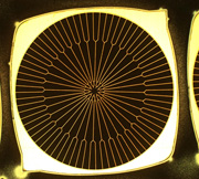 |
| Multi-junction concentrator solar cell with an efficiency of 39.7% at a concentration factor of 300, developed at Fraunhofer ISE. |
Abstract:
LayTec GmbH of Berlin, Germany says that the German Federal Ministry of Economics and Technology (Bundesministerium für Wirtschaft und Technologie) has approved funding within the PRO Inno Program for the development of a new in-situ sensor for the photovoltaic market.
LayTec to develop in-situ sensor for ISE’s triple-junction PV cells
Berlin, Germany | Posted on October 6th, 2008 In collaboration with the Fraunhofer Institute for Solar Energy Systems (ISE) in Freiburg, Germany, a research project has been launched to improve the in-situ monitoring of MOCVD processes for triple-junction photovoltaic cells being developed at Fraunhofer ISE (which recently set the European record for solar cell efficiency, at 39.7%). Cooperation between LayTec and ISE's III-V Epitaxy and Solar Cells group is aimed at developing monitoring sensors for industrial-scale manufacturing of triple-junction solar cells with improved process control in multi-wafer MOCVD reactors. "Real-time analysis and control of our processes is becoming a key for the development of complex semiconductor structures such as multi-junction solar cells" says Dr Frank Dimroth, head of ISE's III-V Epitaxy and Solar Cells group.
ISE's cells are the most efficient produced in Europe. ISE transfers its process technology to the cooperation partner Azur Space Solar Power GmbH of Heilbronn, Germany (Azur SSP), which prepares them for commercial production. ISE and Azur SSP use Aixtron Planetary systems for both development and manufacturing. LayTec's EpiCurveTT sensor, which the firm claims is already the bestseller for the MOCVD LED market, will be further improved to achieve the resolution necessary for multi-junction solar cell growth under the conditions of planetary rotation. In addition to temperature, layer thickness and strain measurements, the new sensor aims to determine the composition and help to better understand the reasons for dislocations and strain within the layers. This will help to compensate for strain-induced temperature inhomogeneities, to determine the thickness of individual thin layers and to monitor the composition of critical heterojunctions, says LayTec.
*LayTec has recruited Dr Qi Cao as a sales engineer. After graduating in physics from China's Nanjing University of Science and Technology, Cao undertook research on optical features of nano-structure materials and obtained a PhD in Optical Engineering in 2004, before continuing research on laser transmission characteristics of nano-holes at Germany's Konstanz University and finally focusing on opto-electric features of single molecules at Münster University. Since 2006, she has gained experience in sales and customer support working for Olympus Microscope in the USA.
At LayTec, Cao will be in charge of sales activities mainly in Taiwan and Greater China, and will support customers and distributors worldwide.
####
About LayTec GmbH
LayTec GmbH was founded in 1999 after an initial period of scientific research and development at the Technical University of Berlin. The company was able to draw from a diverse range of scientific knowledge, patents and entrepreneurial experience in the semiconductor industry to position itself as an innovator and dominant brand in the real-time thin-film optical sensor market.
For more information, please click here
Contacts:
Helmholtzstr. 13/14
D-10587 Berlin
Germany
Tel: +49 (0)30 39 800 80-0
Fax:+49 (0)30 39 800 80-80
Copyright © LayTec GmbH
If you have a comment, please Contact us.Issuers of news releases, not 7th Wave, Inc. or Nanotechnology Now, are solely responsible for the accuracy of the content.
Bookmark:


| Related News Press |
News and information
![]() Quantum computer improves AI predictions April 17th, 2026
Quantum computer improves AI predictions April 17th, 2026
![]() Flexible sensor gains sensitivity under pressure April 17th, 2026
Flexible sensor gains sensitivity under pressure April 17th, 2026
![]() A reusable chip for particulate matter sensing April 17th, 2026
A reusable chip for particulate matter sensing April 17th, 2026
![]() Detecting vibrational quantum beating in the predissociation dynamics of SF6 using time-resolved photoelectron spectroscopy April 17th, 2026
Detecting vibrational quantum beating in the predissociation dynamics of SF6 using time-resolved photoelectron spectroscopy April 17th, 2026
Thin films
![]() Tiny nanosheets, big leap: A new sensor detects ethanol at ultra-low levels January 30th, 2026
Tiny nanosheets, big leap: A new sensor detects ethanol at ultra-low levels January 30th, 2026
![]() Utilizing palladium for addressing contact issues of buried oxide thin film transistors April 5th, 2024
Utilizing palladium for addressing contact issues of buried oxide thin film transistors April 5th, 2024
![]() Understanding the mechanism of non-uniform formation of diamond film on tools: Paving the way to a dry process with less environmental impact March 24th, 2023
Understanding the mechanism of non-uniform formation of diamond film on tools: Paving the way to a dry process with less environmental impact March 24th, 2023
![]() New study introduces the best graphite films: The work by Distinguished Professor Feng Ding at UNIST has been published in the October 2022 issue of Nature Nanotechnology November 4th, 2022
New study introduces the best graphite films: The work by Distinguished Professor Feng Ding at UNIST has been published in the October 2022 issue of Nature Nanotechnology November 4th, 2022
Govt.-Legislation/Regulation/Funding/Policy
![]() Quantum computer improves AI predictions April 17th, 2026
Quantum computer improves AI predictions April 17th, 2026
![]() Metasurfaces smooth light to boost magnetic sensing precision January 30th, 2026
Metasurfaces smooth light to boost magnetic sensing precision January 30th, 2026
![]() New imaging approach transforms study of bacterial biofilms August 8th, 2025
New imaging approach transforms study of bacterial biofilms August 8th, 2025
Sensors
![]() Flexible sensor gains sensitivity under pressure April 17th, 2026
Flexible sensor gains sensitivity under pressure April 17th, 2026
![]() Tiny nanosheets, big leap: A new sensor detects ethanol at ultra-low levels January 30th, 2026
Tiny nanosheets, big leap: A new sensor detects ethanol at ultra-low levels January 30th, 2026
![]() From sensors to smart systems: the rise of AI-driven photonic noses January 30th, 2026
From sensors to smart systems: the rise of AI-driven photonic noses January 30th, 2026
![]() Sensors innovations for smart lithium-based batteries: advancements, opportunities, and potential challenges August 8th, 2025
Sensors innovations for smart lithium-based batteries: advancements, opportunities, and potential challenges August 8th, 2025
Announcements
![]() A fundamentally new therapeutic approach to cystic fibrosis: Nanobody repairs cellular defect April 17th, 2026
A fundamentally new therapeutic approach to cystic fibrosis: Nanobody repairs cellular defect April 17th, 2026
![]() UC Irvine physicists discover method to reverse ‘quantum scrambling’ : The work addresses the problem of information loss in quantum computing system April 17th, 2026
UC Irvine physicists discover method to reverse ‘quantum scrambling’ : The work addresses the problem of information loss in quantum computing system April 17th, 2026
Solar/Photovoltaic
![]() Spinel-type sulfide semiconductors to operate the next-generation LEDs and solar cells For solar-cell absorbers and green-LED source October 3rd, 2025
Spinel-type sulfide semiconductors to operate the next-generation LEDs and solar cells For solar-cell absorbers and green-LED source October 3rd, 2025
![]() KAIST researchers introduce new and improved, next-generation perovskite solar cell November 8th, 2024
KAIST researchers introduce new and improved, next-generation perovskite solar cell November 8th, 2024
![]() Groundbreaking precision in single-molecule optoelectronics August 16th, 2024
Groundbreaking precision in single-molecule optoelectronics August 16th, 2024
![]() Development of zinc oxide nanopagoda array photoelectrode: photoelectrochemical water-splitting hydrogen production January 12th, 2024
Development of zinc oxide nanopagoda array photoelectrode: photoelectrochemical water-splitting hydrogen production January 12th, 2024
|
|
||
|
|
||
| The latest news from around the world, FREE | ||
|
|
||
|
|
||
| Premium Products | ||
|
|
||
|
Only the news you want to read!
Learn More |
||
|
|
||
|
Full-service, expert consulting
Learn More |
||
|
|
||