Home > Press > Foldable and stretchable, silicon circuits conform to many shapes
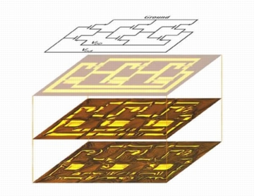 |
| Photo courtesy John Rogers Circuit diagram (top frame) and optical images of a stretchable, "wavy" silicon ring oscillator circuit on a rubber substrate, in the "as fabricated" flat state (top micrograph) and in moderate and high states of biaxial compression (middle and bottom micrographs, respectively). |
Abstract:
Scientists have developed a new form of stretchable silicon integrated circuit that can wrap around complex shapes such as spheres, body parts and aircraft wings, and can operate during stretching, compressing, folding and other types of extreme mechanical deformations, without a reduction in electrical performance.
Foldable and stretchable, silicon circuits conform to many shapes
CHAMPAIGN, IL | Posted on March 27th, 2008"The notion that silicon cannot be used in such applications because it is intrinsically brittle and rigid has been tossed out the window," said John Rogers, a Founder Professor of Materials Science and Engineering at the University of Illinois.
"Through carefully optimized mechanical layouts and structural configurations, we can use silicon in integrated circuits that are fully foldable and stretchable," said Rogers, who is a corresponding author of a paper accepted for publication in the journal Science, and posted on its Science Express Web site.
The new designs and fabrication strategies could produce wearable systems for personal health monitoring and therapeutics, or systems that wrap around mechanical parts such as aircraft wings and fuselages to monitor structural properties.
In December 2005, Rogers and his U. of I. research group reported the development of a one-dimensional, stretchable form of single-crystal silicon with micron-sized, wave-like geometries. That configuration allows reversible stretching in one direction without significantly altering the electrical properties, but only at the level of individual material elements and devices.
Now, Rogers and collaborators at the U. of I., Northwestern University, and the Institute of High Performance Computing in Singapore report an extension of this basic wavy concept to two dimensions, and at a much more sophisticated level to yield fully functional integrated circuit systems.
"We've gone way beyond just isolated material elements and individual devices to complete, fully integrated circuits in a manner that is applicable to systems with nearly arbitrary levels of complexity," said Rogers, who also is a researcher at the Beckman Institute and at the university's Frederick Seitz Materials Research Laboratory.
"The wavy concept now incorporates optimized mechanical designs and diverse sets of materials, all integrated together in systems that involve spatially varying thicknesses and material types," Rogers said. "The overall buckling process yields wavy shapes that vary from place to place on the integrated circuit, in a complex but theoretically predictable fashion."
Achieving high degrees of mechanical flexibility, or foldability, is important to sustaining the wavy shapes, Rogers said. "The more robust the circuits are under bending, the more easily they will adopt the wavy shapes which, in turn, allow overall system stretchability. For this purpose, we use ultrathin circuit sheets designed to locate the most fragile materials in a neutral plane that minimizes their exposure to mechanical strains during bending."
To create their fully stretchable integrated circuits, the researchers begin by applying a sacrificial layer of polymer to a rigid carrier substrate. On top of the sacrificial layer they deposit a very thin plastic coating, which will support the integrated circuit. The circuit components are then crafted using conventional techniques for planar device fabrication, along with printing methods for integrating aligned arrays of nanoribbons of single-crystal silicon as the semiconductor. The combined thickness of the circuit elements and the plastic coating is about 50 times smaller than the diameter of a human hair.
Next, the sacrificial polymer layer is washed away, and the plastic coating and integrated circuit are bonded to a piece of prestrained silicone rubber. Lastly, the strain is relieved, and as the rubber springs back to its initial shape, it applies compressive stresses to the circuit sheet. Those stresses spontaneously lead to a complex pattern of buckling, to create a geometry that then allows the circuit to be folded, or stretched, in different directions to conform to a variety of complex shapes or to accommodate mechanical deformations during use.
The researchers constructed integrated circuits consisting of transistors, oscillators, logic gates and amplifiers. The circuits exhibited extreme levels of bendability and stretchability, with electronic properties comparable to those of similar circuits built on conventional silicon wafers.
The new design and construction strategies represent general and scalable routes to high-performance, foldable and stretchable electronic devices that can incorporate established, inorganic electronic materials whose fragile, brittle mechanical properties would otherwise preclude their use, the researchers report.
"We're opening an engineering design space for electronics and optoelectronics that goes well beyond what planar configurations on semiconductor wafers can offer," Rogers said.
The work was funded by the National Science Foundation and the U.S. Department of Energy.
####
About University of Illinois
At Illinois, research shapes the campus identity, stimulates classroom instruction and serves as a springboard for public engagement activities throughout the world. Opportunities abound for graduate students to develop independent projects and launch their own careers as researchers while working alongside faculty and assisting in their research. Illinois continues its long tradition of groundbreaking accomplishments with remarkable new discoveries and achievements that inspire and enrich the lives of people around the world.
For more information, please click here
Contacts:
James E. Kloeppel
Physical Sciences Editor
217-244-1073
Copyright © University of Illinois
If you have a comment, please Contact us.Issuers of news releases, not 7th Wave, Inc. or Nanotechnology Now, are solely responsible for the accuracy of the content.
Bookmark:


| Related News Press |
Govt.-Legislation/Regulation/Funding/Policy
![]() Quantum computer improves AI predictions April 17th, 2026
Quantum computer improves AI predictions April 17th, 2026
![]() Metasurfaces smooth light to boost magnetic sensing precision January 30th, 2026
Metasurfaces smooth light to boost magnetic sensing precision January 30th, 2026
![]() New imaging approach transforms study of bacterial biofilms August 8th, 2025
New imaging approach transforms study of bacterial biofilms August 8th, 2025
Chip Technology
![]() A reusable chip for particulate matter sensing April 17th, 2026
A reusable chip for particulate matter sensing April 17th, 2026
![]() Metasurfaces smooth light to boost magnetic sensing precision January 30th, 2026
Metasurfaces smooth light to boost magnetic sensing precision January 30th, 2026
Announcements
![]() A fundamentally new therapeutic approach to cystic fibrosis: Nanobody repairs cellular defect April 17th, 2026
A fundamentally new therapeutic approach to cystic fibrosis: Nanobody repairs cellular defect April 17th, 2026
![]() UC Irvine physicists discover method to reverse �quantum scrambling� : The work addresses the problem of information loss in quantum computing system April 17th, 2026
UC Irvine physicists discover method to reverse �quantum scrambling� : The work addresses the problem of information loss in quantum computing system April 17th, 2026
Aerospace/Space
![]() Decoding hydrogen‑bond network of electrolyte for cryogenic durable aqueous zinc‑ion batteries January 30th, 2026
Decoding hydrogen‑bond network of electrolyte for cryogenic durable aqueous zinc‑ion batteries January 30th, 2026
![]() ICFO researchers overcome long-standing bottleneck in single photon detection with twisted 2D materials August 8th, 2025
ICFO researchers overcome long-standing bottleneck in single photon detection with twisted 2D materials August 8th, 2025
![]() Onion-like nanoparticles found in aircraft exhaust May 14th, 2025
Onion-like nanoparticles found in aircraft exhaust May 14th, 2025
|
|
||
|
|
||
| The latest news from around the world, FREE | ||
|
|
||
|
|
||
| Premium Products | ||
|
|
||
|
Only the news you want to read!
Learn More |
||
|
|
||
|
Full-service, expert consulting
Learn More |
||
|
|
||