Home > Press > Measurement Innovations Add Up to Big Savings for Semiconductors
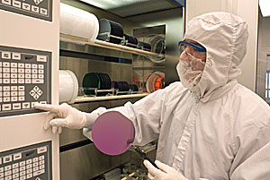 |
| Russell Hajdaj prepares silicon wafers that will be "baked" as part of the processing required for producing new types of semiconductor devices.
Credit: Copyright Robert Rathe |
Abstract:
A new report* from the National Institute of Standards and Technology (NIST) shows that investment in measurement science has and will continue to have a dramatic effect on innovation, productivity, growth and competitiveness in and among high technology sectors. Citing the semiconductor industry as a case in point, the analysis, prepared for NIST by RTI International (RTI), estimates that the $12 billion spent on advancing measurement capabilities during the decade beginning in 1996 will have saved that sector more than $51 billion in scrap and rework costs by 2011—a net benefit of approximately $39 billion.
*Economic Impact of Measurement in the Semiconductor Industry is available on the NIST Web site at http://www.nist.gov/director/planning/policy_studies.htm
Measurement Innovations Add Up to Big Savings for Semiconductors
GAITHERSBURG, MD | Posted on January 9th, 2008RTI estimates that for every dollar spent on measurement, the industry as a whole saw a $3.30 return. (Dollar amounts represent 2006 dollars adjusted for inflation.) The report found that the strategic focus on measurement technologies pursued by the International Technology Roadmap for Semiconductors (ITRS), a consortium of chip manufacturers and related stakeholders, benefited both the industry and consumers through the reduction of defect rates and the miniaturization of feature size. The advances fostered through this effort, among others, resulted in lower costs, higher product quality and ever faster processing speeds.
Measurement technology has allowed the industry to keep up with "Moore's Law," which predicts the number of transistors per chip will double every two years. By the early 1990s, the industry realized it would no longer be possible to satisfy this benchmark without the ability to manipulate nanoscale-sized features. The report credits the initiative to augment nanoscale measurement capabilities outlined in the ITRS and its predecessor as one of the factors that helped manufacturers to increase the possible number of transistors per chip from 3.1 million in 1996 to 1.7 billion in 2006 while making marked improvements in quality, design, software and interoperability.
The report underlines the importance of measurement science to the semiconductor industry and highlights several areas that need further improvement if the industry is to stay on pace. These areas include the need for new standards for measuring features lengths at 32 nanometers, new techniques for controlling radio-frequency electromagnetic energy and high-frequency magnetic fields, and better chemical and materials standards, as well as new and more accurate calibration, interoperability and test standards.
RTI gathered the information for this analysis through surveys and other means. The answered queries accounted for more than 80 percent of the semiconductor industry, and the results were taken to be representative of the industry as a whole. The results may also be viewed as conservative in that RTI was able to quantitatively estimate productivity impacts but not increases in quality.
####
About NIST
Founded in 1901, NIST is a non-regulatory federal agency within the U.S. Department of Commerce. NIST's mission is to promote U.S. innovation and industrial competitiveness by advancing measurement science, standards, and technology in ways that enhance economic security and improve our quality of life.
For more information, please click here
Contacts:
Mark Esser
(301) 975-2767
Copyright © NIST
If you have a comment, please Contact us.Issuers of news releases, not 7th Wave, Inc. or Nanotechnology Now, are solely responsible for the accuracy of the content.
Bookmark:


| Related News Press |
News and information
![]() Quantum computer improves AI predictions April 17th, 2026
Quantum computer improves AI predictions April 17th, 2026
![]() Flexible sensor gains sensitivity under pressure April 17th, 2026
Flexible sensor gains sensitivity under pressure April 17th, 2026
![]() A reusable chip for particulate matter sensing April 17th, 2026
A reusable chip for particulate matter sensing April 17th, 2026
![]() Detecting vibrational quantum beating in the predissociation dynamics of SF6 using time-resolved photoelectron spectroscopy April 17th, 2026
Detecting vibrational quantum beating in the predissociation dynamics of SF6 using time-resolved photoelectron spectroscopy April 17th, 2026
Chip Technology
![]() A reusable chip for particulate matter sensing April 17th, 2026
A reusable chip for particulate matter sensing April 17th, 2026
![]() Metasurfaces smooth light to boost magnetic sensing precision January 30th, 2026
Metasurfaces smooth light to boost magnetic sensing precision January 30th, 2026
Announcements
![]() A fundamentally new therapeutic approach to cystic fibrosis: Nanobody repairs cellular defect April 17th, 2026
A fundamentally new therapeutic approach to cystic fibrosis: Nanobody repairs cellular defect April 17th, 2026
![]() UC Irvine physicists discover method to reverse ‘quantum scrambling’ : The work addresses the problem of information loss in quantum computing system April 17th, 2026
UC Irvine physicists discover method to reverse ‘quantum scrambling’ : The work addresses the problem of information loss in quantum computing system April 17th, 2026
|
|
||
|
|
||
| The latest news from around the world, FREE | ||
|
|
||
|
|
||
| Premium Products | ||
|
|
||
|
Only the news you want to read!
Learn More |
||
|
|
||
|
Full-service, expert consulting
Learn More |
||
|
|
||