Home > Press > Made in IBM Labs: 10 Chip Breakthroughs in 10 Years
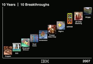 |
| 10 IBM Breakthroughs in 10 Years -- Beginning with the use of copper for chip wiring, IBM has announced 10 semiconductor innovations over the course of 10 years that have enabled computers and many other kinds of electronic devices to become smaller, less expensive, more powerful, and more energy efficient. IBM today announced it has harnessed the natural tendency of materials to form patterns to create a vacuum between the miles of wires inside chips. This provides better insulation speeding performance and reducing power consumption. |
Abstract:
Today's announcement by IBM (NYSE: IBM) of a major breakthrough in chip design -- called "airgap" -- bookends a decade of innovation from IBM Labs that have transformed the IT industry with new materials and design architectures to build smaller, more powerful and energy efficient chips.
Made in IBM Labs: 10 Chip Breakthroughs in 10 Years
ARMONK, NY | Posted on May 3rd, 2007IBM's pioneering work to move the industry from aluminum to copper wiring, unveiled in 1997, gave the industry an immediate 35 percent reduction in electron flow resistance and a 15 percent boost in chip performance.
Since then, IBM scientists have continued to drive performance improvements to continue the path of Moore's Law. Ten of IBM's biggest chip breakthroughs chosen from the dozens of innovations coming from IBM's labs in the past ten years include:
1. Copper (September 1997) -- Replacing aluminum wiring in chips had been thought by most to be impossible, for a number of technical reasons. An IBM team overcame those technical problems, bringing copper wires into production quickly, giving an immediate boost to chip performance. IBM's pioneering techniques are now the industry standard.
2. SOI (August 1998) -- Silicon on Insulator technology reduces power consumption and increases performance by helping insulate the millions of transistors on modern chips. The industry had been working on this technology for 15 years before IBM made it happen.
3. Strained Silicon (June 2001) -- This technology stretches the material inside chips, decreasing the resistance and speeding the flow of electrons through transistors to increase performance and decrease power consumption.
4. Dual-Core Microprocessors (October 2001) -- POWER4, the world's first dual-core microprocessor, was announced as part of Regatta, a System p server and the world's most powerful. More than two years would pass -- an eternity in the technology business -- before our first competitors brought a dual-core chip to market.
5. Immersion Lithography (December 2004) -- IBM announces it is the first company in the world to use this new manufacturing technology -- a method to build chips with ever smaller features -- to produce commercial microprocessors.
6. Frozen SiGe Chip (June 2006) -- In the 1990s, IBM first uses Silicon Germanium to replace more expensive and exotic materials, leading to smaller, faster and lower cost chips, and pushing IBM into the business of selling chips to companies for wireless products, such as mobile phones and routers. Last year, IBM pushed the limits of its SiGe technology again when it teamed with Georgia Tech -- with support from NASA -- to demonstrate the first silicon-based chip capable of operating at frequencies above 500GHz, by "freezing" the chip to near absolute zero.
7. High-k (January 2007) -- IBM announces a solution to one of the industry's most vexing problems -- transistors that leak current. By using new materials IBM will create chips with "high-k metal gates" that will enable products with better performance that are both smaller and more power efficient.
8. eDRAM (February 2007) -- By replacing SRAM with an innovative new type of speedy DRAM on a microprocessor chip, IBM will be able to more than triple the amount of embedded memory and boost performance significantly.
9. 3-D Chip Stacking (April 2007) -- IBM announces the creation of three-dimensional chips using "through-silicon vias," allowing semiconductors to be stacked vertically instead of being placed near each other horizontally. This cuts the length of critical circuit pathways by up to 1,000 times.
10. Airgap (May 2007) -- Using a "self assembly" nanotechnology IBM has created a vacuum between the miles of wire inside a Power Architecture microprocessor reducing unwanted capacitance and improving both performance and power efficiency.
####
About IBM
Note to Editors:
Broadcast-quality video on airgap can be downloaded by journalists at: http://www.thenewsmarket.com/ibm.
Photos and related materials are available in the IBM Press Room at: http://www-03.ibm.com/press/us/en/presskit/21463.wss.
For further information about IBM Microelectronics, visit http://www.ibm.com/chips/
For more information about IBM Research, visit http://www.ibm.com/research
For more information, please click here
Contacts:
Bruce McConnel
IBM Media Relations
914-766-4427 (o)
203-739-5462 (m)
Copyright © Market Wire
If you have a comment, please Contact us.Issuers of news releases, not 7th Wave, Inc. or Nanotechnology Now, are solely responsible for the accuracy of the content.
Bookmark:


| Related News Press |
Chip Technology
![]() A reusable chip for particulate matter sensing April 17th, 2026
A reusable chip for particulate matter sensing April 17th, 2026
![]() Metasurfaces smooth light to boost magnetic sensing precision January 30th, 2026
Metasurfaces smooth light to boost magnetic sensing precision January 30th, 2026
Announcements
![]() A fundamentally new therapeutic approach to cystic fibrosis: Nanobody repairs cellular defect April 17th, 2026
A fundamentally new therapeutic approach to cystic fibrosis: Nanobody repairs cellular defect April 17th, 2026
![]() UC Irvine physicists discover method to reverse �quantum scrambling� : The work addresses the problem of information loss in quantum computing system April 17th, 2026
UC Irvine physicists discover method to reverse �quantum scrambling� : The work addresses the problem of information loss in quantum computing system April 17th, 2026
Human Interest/Art
![]() New 2D multifractal tools delve into Pollock's expressionism January 17th, 2025
New 2D multifractal tools delve into Pollock's expressionism January 17th, 2025
![]() Drawing data in nanometer scale September 30th, 2022
Drawing data in nanometer scale September 30th, 2022
![]() Scientists prepare for the world�s smallest race: Nanocar Race II March 18th, 2022
Scientists prepare for the world�s smallest race: Nanocar Race II March 18th, 2022
![]() Graphene nanotubes revolutionize touch screen use for prosthetic hands August 3rd, 2021
Graphene nanotubes revolutionize touch screen use for prosthetic hands August 3rd, 2021
|
|
||
|
|
||
| The latest news from around the world, FREE | ||
|
|
||
|
|
||
| Premium Products | ||
|
|
||
|
Only the news you want to read!
Learn More |
||
|
|
||
|
Full-service, expert consulting
Learn More |
||
|
|
||