Home > Nanotechnology Columns > NanoGlobe > Singapore's Capability in Atomic Layer Deposition
 |
NanoGlobe Pte Ltd Nanotechnology Business Development Consultants NanoGlobe Pte Ltd |
Abstract:
Precise control of film thickness in atomic scale and uniform coverage over intricate substrate are a few of advantages possessed by atomic layer deposition (ALD) technology, making it recently more favourable as compared to other deposition techniques. Scientists in institute of Materials Research and Engineering (IMRE) in Singapore have successfully acquired the know-how in developing affordable ALD equipment for more effective commercialization. Led by Dr GAO Han, ALD technology development in IMRE has progressed further to applying ALD in fabricating well aligned and controlled TiO2 nanotube arrays for photocatalytic applications, gas sensing device for example. We share in this article our interview with Dr Gao about his research exciting activities.
July 9th, 2010
Singapore's Capability in Atomic Layer Deposition
Atomic scale, atomic precision, atomic layer deposition. Invented in 1974 by a Finnish scientist, Atomic Layer Deposition (ALD) is a method to apply a very thin and conformal film or coating onto various substrates based on sequential self limiting surface reactions - gas phase chemical process, to control the growth of the film. The name itself suggests thickness ability to be as fine as atomic scale per monolayer.
ALD technology has currently been receiving increasing attention commercially due to its advantages compared to other deposition methods. It provides extremely good control of film thickness and compositions, involves lower deposition temperatures than other chemical deposition methods, resulting in pinhole-free and conformal film, and is an easy technique for batch processing. It is also scalable and can be done roll to roll by some of the industry players such as Beneq.
Institute of Materials Research and Engineering (IMRE) in Singapore is one of many organizations that have been going deep in researching and developing ALD technology for nanofabrication application. On 15 June 2010, NanoGlobe team had the opportunity to interview Dr GAO Han, the Principal Investigator of ALD in IMRE. Working together with his teammates in Patterning & Fabrication Group, Dr Gao has successfully developed and transferred the cost effective know-how of IMRE ALD technology in 2008 to a Singapore company, Azimuth Technologies Pte Ltd, to commercialize the-now-affordable ALD instrumentation and be the only company in South East Asia with this capability. Dr Gao showed us his in-house assembly of ALD equipment, which is pretty impressive to us due to its simplicity yet powerful capability in yielding remarkable results. His in-house equipment has been tested to be capable of producing TiO2, SiO2 and ZnO.
The most recent achievement published by Dr Gao's team was the fabrication of transparent and well aligned TiO2 nanotube arrays with controllable dimensions for photocatalytic applications. His group has successfully produced standing TiO2 nanotubes with sufficiently thin wall for good transparency yet thick enough for excellent photocatalytic activity - minimum recombination of the electron-hole pairs generated by UV irradiation. This result was attributed to the capability of ALD technique for atomic layer growth and conformal thin films, as well as the use of free-standing highly ordered porous anodic alumina template, another in-house capability developed by Dr Gao. His team is capable of producing TiO2 nanotubes height of 200nm and wall thickness of 15nm in average. This structure of TiO2 nanotube arrays will be effective, for example as gas sensing device. TiO2 nanotubes instead of TiO2 film are preferred due to larger surface area, therefore maximizing the contact with the target species to be sensed.
Before joining IMRE in 2003, Dr Gao spent his early years in China, including his Doctoral study in Zhejiang University and Postdoctoral study in Peking University. He initially worked on the fabrication of nanoporous anodic alumina template with electrodeposition technique before embarking on developing ALD technology in 2005 and since then he has been focusing on developing and applying ALD for nanofabrication and device integration. Besides nanofabrication that involves ALD and anodic alumina, his research interests also include template-assisted growth of nanomaterials and nanoarrays-based chemical & biosensors.
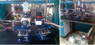 |
| IMRE�s in-house assembly of ALD equipment |
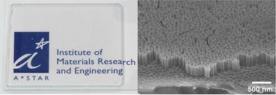 |
| The sample glass substrate (left), covered with Pd-functionalised TiO2 nanotube arrays, is uniform and optically transparent, and gives a clear view of the A*STAR logo beneath. The TiO2 nanotube arrays are well-aligned, highly ordered, and firmly attached onto the glass substrate as can be seen from the scanning electron microscope image (right) with a scale bar of 500 nm. The nanotube wall thickness can be precisely controlled using ALD and made to be sufficiently thin so that it is transparent but thick enough to have excellent photocatalytic properties (Source: Dr Gao Han, IMRE Singapore) |
Bookmark:


|
|
||
|
|
||
| The latest news from around the world, FREE | ||
|
|
||
|
|
||
| Premium Products | ||
|
|
||
|
Only the news you want to read!
Learn More |
||
|
|
||
|
Full-service, expert consulting
Learn More |
||
|
|
||