Home > Nanotechnology Columns > NanoGlobe > Nanotechnology and A*STAR Printable Electronics Research Workshop
 |
NanoGlobe Pte Ltd Nanotechnology Business Development Consultants NanoGlobe Pte Ltd |
Abstract:
Printable electronics, which is a relatively new field for producing thin, flexible and cheap electronic devices, is on the rise with many research activities devoted to develop further new materials, new processes, and device fabrication and integration. Singapore research funding agency A*STAR launched in 2006 the Polymer and Molecular Electronics and Devices (PMED) aiming to build competencies in plastic electronics and stimulate printed electronics industry development in Singapore. Printable electronics workshop organized by the Institute of Materials Research and Engineering (IMRE) of A*STAR discussed some of the latest research progress in organic electronics that is part of PMED's projects, including promising dielectric materials for organic thin film transistors and new low bandgap polymers for organic photovoltaics. In addition, some preparations required for commercialization of printable electronics especially in large scale were presented and elaborated.
January 21st, 2010
Nanotechnology and A*STAR Printable Electronics Research Workshop
To kick off 2010 research outreach activities, the Institute of Materials Research and Engineering (IMRE) in Singapore organized on 8 January a workshop focusing on Printable Electronics research topic. In this workshop, R&D projects and progress that are part of the Polymer and Molecular Electronics and Devices (PMED) programme were presented. PMED is one of the funded programmes under Thematic Strategic Research Programme of A*STAR Singapore (Agency for Science, Technology and Research), aiming to build competencies in plastic electronics, develop critical component technologies for PMED for enabling design of low-cost, high-value electronic devices, and simulate printed electronics industry development that will contribute to the creation of a knowledge-based economy in Singapore. As explained by PMED TSRP Director, Dr Beng Ong, PMED applies a holistic approach from the fundamental studies, materials and materials processes to devices and device integration. Since February 2006, it has received industry support of more than S$3M to fund the projects and collaborates with five industry partners, outperformed the expected target which was only S$0.5M and zero industry partners, respectively.
The workshop mainly presented the technical details of research progress and results including new materials synthesis, transport mechanisms, new materials properties, new fabrication process, and device characterization and optimization. Substantial time is devoted to develop solution processable materials for dielectrics and low band gap polymers for OPV application. For example, oleic acid-capped perovskite(e.g. BaTiO3, SrTiO3) nanoparticles exhibit high k value (4-12) making them promising materials for dielectric application for organic thin film transistors. As explained by Dr Mary Chan, Associate Professor in Nanyang Technological University, the nanoparticles suspensions are stable due to the presence of oleic acid, and therefore they be processed with simple spin-coating and printing method. Dr Chen Zhikuan, Senior Scientist at IMRE, shared a series of new low bandgap polymers, promising for organic photovoltaics application. He showed that the new polymers (based on phenyl butyric acid methyl ester) are capable of producing power conversion efficiency of more than 5%.
Another interesting topic presented was the commercialization aspect of printed electronics. Delivered by Dr Daniel Gamota, the co-founder and principal of Printovate Inc., the commercialization preparation of all-printed large area electronics devices requires well established standards, testing methodology and operating procedures to ensure robust manufacturing processes and high yield of final products. Similar to any other devices manufacturing, printed electronics industry must establish a smooth supply chain, common understanding of product quality control and assurance, and in-line process control. We have to recognize many factors that contribute to the yield of final products, such as materials compatibility, ink particle size effect, substrate wetting properties, circuit design and simulation, etc. We also have to establish the right tests and analysis such as temperature cycle, thermal shock, aging and flexure test, to ensure sufficient device reliability for ensuring customers satisfaction. In addition, the International Electronics Manufacturing Initiative (INEMI, www.inemi.org) has engaged printers and printing equipment, electronics equipment and materials suppliers to build supply chain based roadmap for large area printed electronics, consisting of more than 110 participants.
The workshop was very informative for participants to know the progress of R&D in printable electronics. It was also important for the industry players to know the prospect and crucial efforts to commercialize and establish a printable electronics industry.
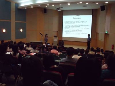 |
| Q&A session after the first technical talk delivered by Prof. Ananth Dodabalapur from the University of Texas, Austin |
Bookmark:


|
|
||
|
|
||
| The latest news from around the world, FREE | ||
|
|
||
|
|
||
| Premium Products | ||
|
|
||
|
Only the news you want to read!
Learn More |
||
|
|
||
|
Full-service, expert consulting
Learn More |
||
|
|
||