Home > Nanotechnology Columns > UAlbany College of Nanoscale Science and Engineering > CMOS-Nano Hybrid Research of CNSE NanoDesign and Modeling Group
 |
Wei Wang Assistant Professor and Senior Research Scientist of Nanoscale Engineering UAlbany- College of Nanoscale Science & Engineering |
Abstract:
Abstract:
The marriage of nanotechnology and CMOS technology will lead to CMOS-nano hybrid technology, which can dramatically advance the development of future integrated circuits (ICs). The CNSE NanoDesign and Modeling (NDM) Group has made new progress in developing CMOS-nano hybrid technologies including the development of new interconnect-based CMOS-hybrid circuits and new reconfigurable structures utilizing nanojunction devices. These new methods open new opportunities to build next generation ICs and are expected to have a huge impact to world-wide IC industries.
July 25th, 2008
CMOS-Nano Hybrid Research of CNSE NanoDesign and Modeling Group
The future of the hundred-billion dollar semiconductor industry relies on the development of novel nanoelectronic devices, circuits and design approaches. Instead of completely replacing CMOS technology, non-conventional nanotechnology is expected to be hybrid with the CMOS systems. Such CMOS-nano hybrid systems try to utilize the advantages of both traditional CMOS devices and novel nanowire/nanotubes materials, which will enhance IC performances in the near future, and create breakthroughs in the long run.
The CNSE NanoDesign and Modeling (NDM) Group has carried out pioneer research in developing new CMOS-nano hybrid technologies. The new results are in two directions:
� Development of CMOS-nano hybrid circuits using new nanointerconnect structures
� Building CMOS-nano hybrid reconfigurable structures based on nanojunction devices
Development of CMOS-nano hybrid circuits using new nanointerconnect structures
The move towards nanoscale ICs poses new challenges to on-chip interconnect design. The currently used Cu interconnect is highly susceptible to electro-migration at high current densities and have low reliability in operation. The resistivity of Cu increases with a decrease in dimensions due to electron surface scattering and grain boundary scattering, which leads to a large interconnect delay and a low current density. Therefore, innovative interconnect materials are being extensively studied as next-generation interconnects.
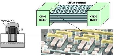 |
| Figure 1: Proposed CMOS-nano IC utilizing carbon nanotubes and graphenes as interconnects. |
The CNSE NDM group developed two carbon-based interconnects, namely, mixed carbon nanotube (CNT) bundle and multi-layer graphene (GNR) interconnects, to be integrated with CMOS to build CMOS-nano ICs. The proposed mixed CNT bundle and multi-layer graphene interconnects show a great performance improvement than Cu. They can sustain a 1000 to 10,000 higher current density than Cu without the problem of electro-migration. They also overcome the high-resistance problem of Cu by offering 2X-3x resistance reduction. Such a performance enhancement will bring many technological breakthroughs in future on-chip interconnects designs. By utilizing these two carbon based interconnects with CMOS devices, the CNSE NDM group developed the CMOS-nano ICs with a significant improvement of interconnect performances. As shown in Figure 1, the proposed IC can utilize carbon nanotube as vias and multi-layer graphene as horizontal wires.
Building CMOS-nano hybrid reconfigurable structures based on nanojunction devices
Another CMOS-nano hybrid structure that the CNSE NDM group developed is based on nanojunction devices. The nanojunction devices are hysteretic resistor junctions that can be used as memory elements. By using such nanodevices as memory and CMOS devices as logic, the proposed CMOS-nano IC can efficiently implement reconfigurable structures such as FPGAs.
The CNSE NDM group developed a number of new CMOS-nano hybrid FPGA structures such as rFPGA and neuroFPGA. The rPGA utilizes the resistive nanojunctions as routing elements and memories in FPGA, which shows 2X-3X performance improvement over the CMOS FPGA. The neuroFPGA utilizes nanojunction with CMOS analog neuromorphic circuits, which provides a new way to build human brain-like computing paradigm. Figure 2 shows the proposed CMOS-nano FPGA utilizing nanojunction devices.
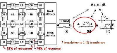 |
| Figure 2: Proposed CMOS-nano FPGA utilizing nanojunction devices. |
This exciting research of CNSE NDM group will definitely accelerate the research in CMOS-nano hybrid technology and the development of IC industry. The CNSE NDM group is working closely with many nanoresearchers to identify challenges and opportunities where nanoscience and nanotechnology can be utilized to advance future IC research.
Bookmark:
http://www.albany.edu/facultyresearch/nanodesign_group/
Bookmark:


|
|
||
|
|
||
| The latest news from around the world, FREE | ||
|
|
||
|
|
||
| Premium Products | ||
|
|
||
|
Only the news you want to read!
Learn More |
||
|
|
||
|
Full-service, expert consulting
Learn More |
||
|
|
||