Home > Nanotechnology Columns > Kos Galatsis > Nanotechnology: a worldwide snapshop.
 |
Kos Galatsis Chief Operating Officer FENA and WIN Centers, UCLA |
Abstract:
I am currently in Japan, attending the 4th International Nanotechnology Conference on Communication and Cooperation. The conference has the unique mission in bringing together US, EU and Asian players to highlight and spur collaboration in nanotechnology. Considering my attendance and participation, what better act than to provide you with a passdown.
April 24th, 2008
Nanotechnology: a worldwide snapshop.
Although I have been to Japan numerous times, I am always pleasantly surprised. The surroundings welcome me with impeccable cleanliness and tidiness, organization, warm hospitality, and well refined aesthetics. It immediately made me wonder how such Japanese cultural traits have heavily contributed to the world's nanotechnology progress with the invention of the Esaki Diode (Leo Esaki, Nobel prize in 1973), use of quantum dots in lasers (Arakawa and Sakaki, 1981) and the discovery of carbon nanotubes (Iijima, 1991). Furthermore, Japan is the technology leader in LED, photocatalyst and Li-ion battery development.
Although Japan is a major player in nanotechnology development, the US still leads nanotechnology funding and the production of scientific journal papers (see Fig 1). China however, just like its sky high GDP growth, is quickly producing a large amount of nanotechnology peer reviewed papers, and if extrapolated, will surpass the US in the coming years (Fig 1).
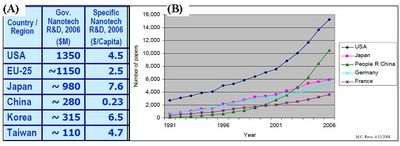 |
| Fig.1: (a) Funding of nanotech by region (b) Publication # in nanotech. [M.Roco-INC4] |
An indicator of nanotechnology leadership and innovation can also be taken by the number of registered patents in each region as shown in Fig 2a. Normalizing the data to "per capita" would make Japan the front runner. However, if we break down the institutional citation rankings in "material science" (Fig 2b), one unravels that the China Academy of Science's leads the race in quantity. But when presenting the data (Fig 2c) on an aggregate, M. Rocco shows that the US leads rankings in nanotechnology papers published in Science, Nature and PNAS.
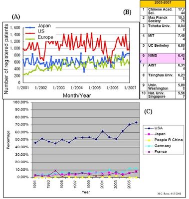 |
| Fig.2: (a) Patent #, (b) mat.sci. citation rankings (c) nano paper rankings |
There were various thrusts discussed and presented, and not surprising, in line with major societal, geopolitical and international themes currently making news. For instance, energy was discussed focusing on energy generation (solar cells) and storage (fuel cells). Sharp presented their new area of solar cells research using dye-sensitized materials. These cells are unique as they mimick photosynthesis, using TiO2 nanoparticles, dyes and electrolyte. Although these cells produce a modest 11% efficiency they are still plagued with practical challenging such as electrolyte leakage and cell stability due to TiO2 - dye interactions. Harry Atwater from Caltech also highlighted his solar cell research in using Si nanowires in order to reduce Si quantity (as its cost has increased due to dramatic Si solar cell demand increase) and also advocated using plasmonics to confine solar energy and reduce film thickness in solar devices.
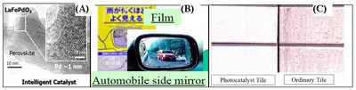 |
| Fig.3: (a) Pd-perovskite (b) hydrophilic mirror (c) clean-tech tile [Seaki,Tanaka-INC4] |
Another major area was nanomaterials. Many nanomaterials make use of rare earth metals such as Pd and Pt, noting their commodity spot prices have increased many times over the past 12 months. These metals are important for catalytic applications such as automobile catalytic converters. The challenge is in increasing efficiency, reducing metal quantity (cost), increasing lifetime and decreasing their operating temperature. The Daihatsu Corporation (Japan) has met this call by engineering intelligent Pt-perovskite nanomaterials as shown in Fig 3a. Conventional catalysts deteriorate via grain growth, but Pt-perovskite materials reside within a perovskite structure making them more stable, increasing lifetime and making use of less Pt metal compared to conventional means. This innovation has been responsible for over 3.5 million vehicles achieving the Super Ultra Low Emission Vehicle (SULEV) standard. Other Japanese companies such as TORAY are using photocatalytic particles for photo induced hydrophilic induction. Applications include hydrophilic automobile mirrors (Fig 3b) and self cleaning tiles (Fig 3c).
 |
| Fig.4: Complimentary CMOS based alternatives presented at INC4 [Thies, Watanabe-INC4] |
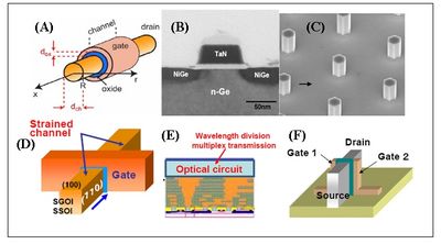
Another major theme was nanoelectronics, in particular focusing on new memory and logic devices. Groups such as Selete, Toshiba and IBM and Intel presented various technologies that are being investigated in pushing CMOS to its limits as shown in Figure 4. Solutions included use of (a) nanowire FETs to achieve ultimate electrostatic control of channel carrier depletion, (b) Ge based FET with shallow source/drain to mitigate short channel effects, (c) III-V nanowire on Si solutions, (d) strained channel FINFETs, (e) optical based interconnect solutions and (f) 4 terminal FET structures and geometries.
However going beyond CMOS was discussed with more vigor and need. The challenges that face nanoelectronics, in particular the search for a new logic and memory device was summarized via six research needs, these include the search for 1) New state variables other than charge (to reduce energy), 2) devices that operate out of equilibrium with the thermal bath (to reduce noise and energy), 3) information transfer mechanisms that are not electromagnetic in nature (for interconnection purposes), 4) phonon engineering for advanced thermal management (to improve heat dissipation) 5) directed self-assembly (to reduce cost) and 6) emerging architectures (for higher functionality). A variety of technologies as shown in Fig. 5 highlight technologies that target these research vectors. Some of these include a) new state variables such as phase change devices, b) new switched that exhibit high Ion/Ioff, c) ballistic based transistors using graphene, d) spin based devices that can incorporate both memory and logic functionality e) quantum dot based floating gate memory devices and (f) high efficiency light emitting diodes using exotic III-V materials.
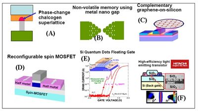 |
| Fig.5: Alternative technologies presented at INC4 [Watanabe-INC4] |
In conclusion, a serious research and development effort exists that spans various areas of nanotechnology. As an example towards nanoelectronics, Japan's nanoelectronic research and development is funded via NEDO (New Energy and Industrial Technology Development Organization), MEXT (Ministry of Education, Culture, Sports, Science and Technology) and Selete which is supported by most of Japan's semiconductor companies. In the US, various organizations, in particular the Focus Center Research Program (FCRP) and the Nanoelectronics Research Initiatives (NRI) are focusing on beyond CMOS research including industrial research organizations supported by research from the DoD, DOE, NSF, NASA and NIST. In Europe, various local, state and EU initiatives exists such as the ENIAC, IST nanoelectronics and NMP programs. The conference provided a means to communicate current and planned activities of nanoelectronics around the world, in particular the pressing needs and technological challenges that require to be overcome. However, more difficult to access and plan was for is cooperation between various regions to leverage expertise and resources in nanotechnology. Some notable examples include the International Planning Working Group for Nanoelectronics which has highlighted some common areas of collaboration to include a) nanotoxicology, b) graphene devices c) magnetic tunnel junctions among others.
The next International Nanotechnology Conference on Communication and Cooperation will be held at UCLA, Los Angeles, May 18th - 21st, 2009.
Bookmark:


|
|
||
|
|
||
| The latest news from around the world, FREE | ||
|
|
||
|
|
||
| Premium Products | ||
|
|
||
|
Only the news you want to read!
Learn More |
||
|
|
||
|
Full-service, expert consulting
Learn More |
||
|
|
||