Home > Nanotechnology Columns > Kos Galatsis > Glorious Graphene - the next nano wonder material
 |
Kos Galatsis Chief Operating Officer FENA and WIN Centers, UCLA |
Abstract:
Extraordinary advances in graphene are now being reported on a daily basis. For good reason. Graphene boasts the most remarkable electronic properties ever to be discovered, making pundits like me feel bullish. I foresee graphene driving the next electronic revolution beyond Si within the next 5-10 years and becoming a fundamental part of integrated circuits by 2019.
January 18th, 2008
Glorious Graphene - the next nano wonder material
Graphene exhibits the highest electronic quality among all known materials, a profound discovery that occurred less than 4 years ago. Although theorists have known of graphene for over 60 years, the community has been delighted to be able to confirm the materials remarkable electronic properties. New insights continue to be published on a monthly basis in leading scientific publications such as Nature and Science. In doing so, advanced research groups both in academia and industry are making graphene a major part of their technology portfolio, migrating away from III-V semiconductors, nanowires and carbon nanotubes. Structurally, graphene is similar to a carbon nanotube, both made up of a single sheet of carbon atoms.
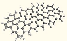 |
| The graphene planar structure - one atom thick sheet of carbon. |
The beauty of graphene is that it is a planar material structure made up of a one-atom-thick sheet of carbon (having 2D simplicity), contrary to carbon nanutubes that are rolled up sheets of graphene, becoming tubes (having 3D complexity). This is a big step forward and probably the most profound advantage that graphene has over CNTs. It was only recently that high flying startups such as Nantero were promising revolutionary electronic CNT based products, but have now been discredited by respectable publications like the IEEE Spectrum magazine, rating the company as "a loser for 2008". In addition to the lack of any measurable commercialization of CNT electronic products, the slow progress more often than not can be traced back to its 3D inferiority complex. A common metric for electronic superiority is electron mobility, which describes the movement of electrons in a material under the influence of an electric field. Graphene has an astonishing 200,000 cm2/Vs which is over 100 times that of silicon. Such high electron mobility lends it to be an extremely efficient conductor and also lends it to be used for high performance devices for both high power (power FETs) and low power (integrated circuit) applications. Graphene also exhibits high gain and high frequency operation in terahertz (THz) frequencies making it useful in analog and RF circuit applications. Other aspects include graphene's exceptional thermal conductivity been measured up to 5850 W/mK (50x more than silicon) quiet possibly making it a superior material for thermal management of nanoscale devices. Graphene has also been shown to be a super sensitive sensor detecting individual gas molecules, reaching ultimate sensor sensitivity. Promising applications include detecting harmful biological and gaseous substances among others.
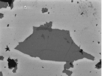 |
| Making graphene is a challenge. State of the art are micron sized samples. |
The most important challenge needed to be resolved is the effective process development of large area growth of graphene. To date, no such wafer scale material or process has so far been developed. Numerous ways to obtain graphene exists but limited to producing micrometer sized (<1μm) "poly crystalline graphene films". Thus, material synthesis is the major bottleneck for realizing high performance graphene devices. Another challenge is in modulating the electronic current that passes through graphene. This is an important aspect of any electronic material, but does not intrinsically exist within graphene. Graphene is a semi-metal, and unfortunately not a semiconductor. Semiconductors are able to be switched both on and off, desirable for logic/memory devices. There are however promising reports indicating ways of getting around this problem. Some solutions include the introduction of double gate structures, quantum confinement via patterning nanoribbons, and implementation of schottky tunnel source and drain devices.
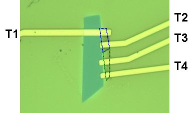 |
| A prototype device based on graphene. |
To summarize, I am bullish on graphene. I foresee the following play:
1. Technology heavy weights such as IBM, HP, GE and DARPA will begin (some already have) to establish serious efforts in targeting synthesis of wafer scale graphene and development of high performance devices (continue up to 2012).
2. Graphene IP applications will exponentially increase, comparable to CNT numbers. Issued patents based on "graphene"=14 compared to "CNT"=448 (continue up to 2016).
3. The VC community will take note and begin directing capital to startups together with an increased SBIR call for graphene based solutions (beginning between 2009-2011).
4. Large cap companies such as Samsung, Intel and Hitatchi and cash rich startups will acquire or license enabling IP from academia and startups that entered in the early stages (beginning between 2012-2015).
5. Highly capitalized development houses and foundries such as SEMATECH, IMEC and LETI will be the first to integrate graphene on Si (beginning between 2014-2017).
6. Small- and mid-cap corporations will begin commercialization of low volume discrete graphene based devices such as sensors and RF components (beginning 2015).
7. Semiconductor manufacturers will then adopted and transfer the technology into their products (beginning 2019).
Bookmark:


|
|
||
|
|
||
| The latest news from around the world, FREE | ||
|
|
||
|
|
||
| Premium Products | ||
|
|
||
|
Only the news you want to read!
Learn More |
||
|
|
||
|
Full-service, expert consulting
Learn More |
||
|
|
||