Home > Nanotechnology Columns > FEI > Overcoming Challenges in Advanced Semiconductor Imaging & Analysis
 |
Dan Fineberg FEI Global Marketing Manager, NanoElectroincs FEI Company |
Abstract:
Time is Money in Nano-scale Semiconductor Manufacturing
Today's advanced semiconductors are truly nano-scale devices. For example, the latest generally-available PC processors feature transistor line-widths as small as 45 nm, and process development is underway at leading manufacturers for 32 nm, 22 nm, and even smaller geometries.
The adage, "Time is money" has an overwhelming relevance in the world of volume semiconductor production. Getting to market, enhancing yields and ramping to volume-- faster-- is business-critical, and overcoming the associated nano-scale manufacturing challenges requires sophisticated "forensics." In other words, advanced manufacturing process development and control applications require advanced imaging and analysis tools to characterize defects, analyze failures, and measure critical dimensions.
December 18th, 2007
Overcoming Challenges in Advanced Semiconductor Imaging & Analysis
Time is Money in Nano-scale Semiconductor Manufacturing
Today's advanced semiconductors are truly nano-scale devices. For example, the latest generally-available PC processors feature transistor line-widths as small as 45 nm, and process development is underway at leading manufacturers for 32 nm, 22 nm, and even smaller geometries.
The adage, "Time is money" has an overwhelming relevance in the world of volume semiconductor production. Getting to market, enhancing yields and ramping to volume-- faster-- is business-critical, and overcoming the associated nano-scale manufacturing challenges requires sophisticated "forensics." In other words, advanced manufacturing process development and control applications require advanced imaging and analysis tools to characterize defects, analyze failures, and measure critical dimensions.
Using the Right Tool for the Job
Scanning electron microscope (SEM) tools have been used for top-down imaging and analysis applications for many years. To get deeper, focused ion beam (FIB) tools are used to cross-section samples for SEM imaging and analysis in three dimensions. To improve the efficiency and effectiveness of those applications, FEI invented DualBeam� platforms, with SEM and FIB columns, more than a decade ago.
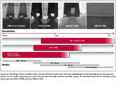
But as geometries shrink, new application methods, tools and techniques are entering the fray. Transmission Electron Microscope (TEM) and Scanning TEM (STEM) tools can reach far higher resolutions than traditional SEM tools. In fact, FEI recently announced that its top-of-the-line Titan� TEM platform has achieved 0.5 Angstrom resolution (just over half the diameter of a Hydrogen atom). Such atomic-scale imaging is now required for a growing range of advanced semiconductor manufacturing process development and control applications -- crystal strain analysis is one of many examples. Today, a range of SEM, STEM and TEM platforms can be found in most advanced semiconductor labs (see figure 1, below).
 |
The Sample Preparation Challenge
The main challenge of STEM and TEM imaging and analysis is the time and cost of preparing samples (known as "lamellas"). Such delays can slow a manufacturer's ramp to volume production, and that can profoundly affect semiconductor profit margins.
STEM and TEM imaging require very thin lamellas because the electron beam must pass through the sample (as opposed to SEM imaging where the electrons bounce off the sample surface). DualBeam tools speed-up lamella preparation compared to old-fashioned mechanical techniques -- the ion beam allows you to finely slice the sample while the SEM allows you to watch while you work.
But leading vendors like FEI are working on improving lamella preparation even further, with the ultimate goal of making STEM and TEM imaging and analysis as rapid and affordable as SEM imaging and analysis (but with all the high-resolution and high-contrast advantages that STEM and TEM platforms deliver).
Future Solutions
Two key areas of innovation are addressing the sample preparation challenge: (1) automating workflow bottlenecks in lamella preparation, imaging and analysis; (2) improving the low kV resolution of next-generation SEM platforms.
Automating workflow bottlenecks can include software applications that execute "recipes" for preparing specific types of lamellas. FEI offers such software today with several DualBeam platforms. In addition, expect to see innovative hardware devices soon that move lamellas from the preparation platform to the imaging/analysis platform - e.g., that "pluck" lamellas from the DualBeam tool and/or "load" them into the TEM. Of course, to get the most value out of these software and hardware innovations, operators will need documented best practices for application methods and techniques that increase the effectiveness and efficiency of each use case.
SEM innovation is at the other end of the spectrum -- to reduce the number of applications that require STEM or TEM samples. Sub-nanometer resolution on an SEM is now possible, and there will be platforms on the market soon that will deliver on that promise in a reliable, repeatable manner.
Look for more information from FEI in the coming months. Many exciting innovations are on the horizon.
Bookmark:


|
|
||
|
|
||
| The latest news from around the world, FREE | ||
|
|
||
|
|
||
| Premium Products | ||
|
|
||
|
Only the news you want to read!
Learn More |
||
|
|
||
|
Full-service, expert consulting
Learn More |
||
|
|
||