Home > Nanotechnology Columns > Kos Galatsis > Rags to riches - Carbon Nanotubes
 |
Kos Galatsis Chief Operating Officer FENA and WIN Centers, UCLA |
Abstract:
With almost two decades of intensive research in pushing CNT technology from the lab to the commercial world, many of us are still waiting to cash in. Most of us know that CNTs offer properties that few materials will ever match. Fabrication and control schemes that have traditionally smothered CNT progress are now maturing, meaning that a rags to riches story may just be around the corner.
December 13th, 2007
Rags to riches - Carbon Nanotubes
Since the discovery of CNTs by Ijima in the early 1990s and with almost two decades of intensive research, ground-breaking innovations for a wide spectrum of applications are pushing CNT from the laboratory to the commercial world. CNTs offer properties that few materials will ever match. Some of these superior properties include high conductivity, excellent thermal properties and superior mechanical properties. Near term applications and associated companies based on carbon nanotube technology worth looking out for include:
� Non-volatile memory (Nantero)
� Field emission displays (Motorola, Samsung)
� Sensors and Actuators (Nanomix, Nano-Proprietary)
� Thermal management (Fujitsu, Nanoconduction)
� IC Interconnect (Fujitsu, Infineon)
� Scanning probe microscopes (Xidex)
� Random number generator (El-Mul)
� General CNT functionalization (Nanocyl)
� Logic Devices (Unidym, NEC, Intel, Aneeve, IBM)
According to NanoMarkets, carbon nanotubes will create $3.6 billion in new business for the electronics and semiconductor sectors by 2009. It is suspected that Unidym will benefit most if CNT based technologies become ubiquitous. The company's recent merger with Carbon Nanotechnologies has made it the dominant portfolio of carbon nanotube-related patents and is one of the largest manufacturers of carbon nanotubes in the world. As hopes are grand, its no wonder that CNT technology currently remains at the top of the Hype Cycle for semiconductors (Gartner). The figure below highlights the progress of the most interesting and significant semiconductor technologies.
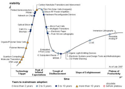 |
| Garner Semiconductor Hype Cycle showing CNT technologies on top. |
More importantly is to understand the dynamics that have contributed to the slow uptake of CNT technology within the commercial playing field. These show stoppers can be summarized as CNT challenges based on:
� Physical Geometry: Their unique 1D structures makes it tricky to manipulate and control tubes. Arranging them in formats such as parallel, intersecting and orthogonal alignment at predetermined locations is extremely difficult particularly with nm precision as is required. Compared to bulk and thin film materials where fabrication occurs from a top-down methodology, CNTs do not offer such a straightforward solution due to their unique 1D geometries. Therefore, incorporating CNT onto most platform such as silicon brings about the classic clash between two competing methodologies; bottom-up vs top-down.
� Growth, Fabrication and Integration Process: Thus far, the growth of nanotubes has been carried out at very high temperatures, and growth below 500�C was seldom. This has made the direct implementation of nanotubes into electronic devices unthinkable. Trying to integrate nanotubes above 400-450 �C would in fact damage the intermetal dielectrics commonly employed in CMOS device fabrication and alter doping profiles. Also, an important practical challenge is the risk of introducing nanotube technology in a clean environment where catalyst metals used to initiate the CNT growth (such as Au) can quickly diffuse into adjacent materials and unnecessarily contaminate the system and associated equipment.
� Chirality and Bandgap Control:
Growing specific metal or semiconducting CNTs is also a process that has not been resolved. Basically, this means that when CNTs are fabricated there is a statistical variation of bandgaps where some tubes are metallic while others are semiconducting. Reducing this variation is key to seeing CNT's being used in mainstream integrated circuits.
� Reproducibility and Sensitivity: High electrical sensitivity is due to the confinement of electrons in the circumferential direction of the tube. Basically this means that anything physically touching or at near proximity induces stress, columbic attraction/repulsion and perturbation of the electron-phonon equilibrium, which ultimately alters the electrical behavior of the tube. Since CNTs typically operate in the ballistic regime (as opposed to the diffusive regime), slight carrier perturbations as a result of the aforementioned reasons will incur in drastic electrical changes to any CNT based system.
With that said, an interesting concept going forward are Silicon-carbon hybrids. Companies such as Nantero are working with LSI Logic Corp to make nanotube RAM using existing silicon processes. Nantero is the first company to actively develop semiconductor products using carbon nanotubes in a production CMOS fab and is also the first company to develop microelectronic-grade carbon nanotube material, compatible with production CMOS fabs. If carbon nanotubes can begin to deliver on their immense potential, investments in companies such as Arrowhead Research (Nasdaq: ARWR) and Harris & Harris (Nasdaq: TINY) could pay significant dividends in the years ahead and become another classic rags to riches story.
Bookmark:


|
|
||
|
|
||
| The latest news from around the world, FREE | ||
|
|
||
|
|
||
| Premium Products | ||
|
|
||
|
Only the news you want to read!
Learn More |
||
|
|
||
|
Full-service, expert consulting
Learn More |
||
|
|
||