Home > Nanotechnology Columns > UAlbany College of Nanoscale Science and Engineering > Nano-optics: Shining a new ‘light' on strained silicon
 |
Robert Geer CNSE Vice President for Academic Affairs and CNSE Chief Academic Officer; Professor of Nanoscale Science University at Albany-College of Nanoscale Science and Engineering |
Abstract:
No field has been impacted by nanotechnology more profoundly than the nanoelectronics industry. ‘Nanochips' play an increasing role in virtually all aspects of our lives - from high-performance computing, communication, and artificial intelligence to the rapidly expanding fields of nanobiology and nanomedicine.
April 13th, 2007
Nano-optics: Shining a new ‘light' on strained silicon
No field has been impacted by nanotechnology more profoundly than the nanoelectronics industry. ‘Nanochips' play an increasing role in virtually all aspects of our lives - from high-performance computing, communication, and artificial intelligence to the rapidly expanding fields of nanobiology and nanomedicine. This widening application base has been enabled by the relentless pursuit of ‘Moore's Law' in continually reducing the feature size and improving the performance of Si-based transistors. These advances come at a price, though. In 1970 the entire ‘chip' industry spent around $100M on R&D (VLSI Research, 2004). Today, the cost of an individual chip fabrication tool is beginning to approach that mark - a case in point is emerging 300mm Si wafer lithography tools that are expected to retail well over $50M each. However, it has taken more than just expensive tools to continually improve the performance of nanochips. Scientists, engineers and designers have turned to materials and processing innovation to make this year's nanochip better than last year's.
One such innovation was the use of so-called ‘strained-Si' for improving transistor performance, first implemented in manufacturing by IBM. The fundamentals of ‘strained-Si' for integrated circuit (IC) chips are straightforward. At some point in our youth we all learn that the mass of an electron is 9.1x10⁻³¹kg. However, in semiconductors conduction electrons ‘act' as if they have a different mass, the so-called effective mass. For example, in Si, the semiconductor of choice for today's chip manufacturers, the effective mass is 8% higher then the ‘bare' mass of an electron. In other words, electrons in Si seem a little ‘heavier' than normal. However, by straining the Si crystal inside a transistor this effective mass can be reduced. In other words, the charge in a Si transistor can be made to move faster (and hence the device works faster - as much as 35% faster) if it is mechanically strained.
This is all well and good. But where does ‘nano' come in? Firstly, engineering the strain across a Si transistor channel 35 nanometers across is no mean feat. Innovations in the processing and fabrication of Si nanodevice structures by companies like IBM, AMD and Intel have made this possible on a routine basis. However, it has resulted in a residual challenge: How can you quickly and reliably measure the strain in a nanoscale Si transistor? There's the hard way - carving out a piece of the transistor and placing it inside a transmission electron microscope (TEM) to measure the distance between the individual silicon atoms. This approach works well but it is extremely time and effort intensive. Hopefully, there will soon be an easier way. Just shine light on it. Specifically, shine light on it and look for a change in the wavelength of the light that is reflected. Some of the photons that are reflected from the silicon give up (or receive) part of their energy to (or from) vibrating silicon atoms. These are called ‘Raman-shifted' photons. In fact, the change in the wavelength of these photons is directly related to the amount of strain in the silicon crystal. So, measuring the strain in silicon devices is as easy as shining light on it.
True, but there's much more to it. Light can only be focused to a spot with a diameter on the order of its wavelength. In other words, a 35 nm channel in a Si transistor will always be much much smaller than the wavelength of light used to measure the Raman shift of reflected photons. And one actually needs to be able to look at individual devices on the chip to accurately characterize the silicon strain. So, we are back to square one. Illuminating a Si device might be a good way to measure Si strain, but one can never get the spatial resolution one needs to look at individual devices.
This is where ‘nano' comes in. There is an elegant way around this limitation. Over the last several years a number of researchers have been working on a phenomena called ‘apertureless' near-field microscopy. In a nutshell this approach can reduce the optical spot size on a surface from many hundreds of nanometers attainable with conventional optical lenses to a few 10s of nanometers. By combining this approach with Raman spectroscopy there is hope that one can use a quick, nondestructive optical approach to measure strain in today's high performance, strained-Si transistors rather than slow and expensive approaches such as TEM. This apertureless approach to optics is a potential boon to nanotechnology where one would needs the power of optical spectroscopy to look at the properties of individual nanostructures.
The fundamental science is straightforward. Illumination of a nanoscale metal particle by the appropriate wavelength light results in collective surface charge oscillations - so-called surface plasmons. The electric field associated with these surface plasmons oscillates at the same frequency of the incident light, but decays exponentially as one moves out from the particle surface. In other words it is strongly localized. If the particle is 10s of nanometers in diameter then the ‘near-field' associated with the surface plasmons is on that some length scale, i.e. a nanoscale-optical spot. By mounting such a particle on the end of a tip of a scanning probe microscope and illuminating it with light this nano-optical spot can be used to collect optical spectra from a nanoscale structure.
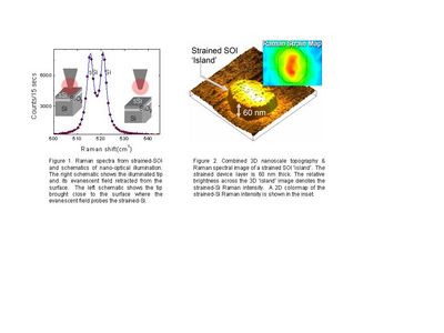
Recently, in our labs at the College of Nanoscale Science & Engineering at the University at Albany, SUNY we have demonstrated the proof-of-feasibility of this approach on large-scale strained-Si test structures. Figure 1 gives a simple schematic of this approach. The test structure consists of a so-called ‘silicon-on-insulator' or SOI stack. This stack separates the Si device layer (top strata) from the bulk Si wafer by a buried silicon oxide layer. For these particular stacks the top Si layer is actually strained to improve charge mobility. The higher strain in the device layer is seen very clearly in the Raman spectra from this structure. Normally there would only be a single peak in the Raman spectrum at 521 cm-1. For the strained SOI stack this peak splits into two (Fig. 1). The Raman peak at lower wavenumber corresponds to the strained Si on the surface. When an illuminated metallic tip is brought within a few nanometers of this surface (left schematic in Fig. 1) the evanescent field of the tip generates Raman-shifted photons. When the tip is retracted (right schematic in Fig. 1) only ‘far-field' Raman-shifted photons are generated. The difference between the Raman spectra for these two tip configurations enables us to generate a nanometer-scale map of the strain.
Such a map of an octagonal strained-Si island or mesa is shown in Fig. 2. The strained Si-Raman signal variation across the mesa is shown in a 2-D color map in the upper left. This data reveals strong variations in the strain across the island. This 2-D map is merged with the island topography in the main portion of the figure. The relative brightness across the 3-D island image denotes the strained-Si Raman peak intensity. This is a first, critical step in the development of a new non-destructive strain metrology for Si-based nanochips and the introduction of nano-optical spectroscopy for a new generation of nanotechnology applications.
 |
Bookmark:


|
|
||
|
|
||
| The latest news from around the world, FREE | ||
|
|
||
|
|
||
| Premium Products | ||
|
|
||
|
Only the news you want to read!
Learn More |
||
|
|
||
|
Full-service, expert consulting
Learn More |
||
|
|
||