Home > Press > Dielectric metalens speed up the development of miniaturized imaging systems
 |
| CREDIT by Meiyan Pan, Yifei Fu, Mengjie Zheng, Hao Chen, Yujia Zang, Huigao Duan, Qiang Li, Min Qiu, and Yueqiang Hu |
Abstract:
Optical lenses have been playing a critical role in imaging systems for plentiful applications such as picture-capturing, sensing, and endoscopy. The developing wearable and portable devices require state-of-the-art imaging devices with higher integration, smaller size, and better performance. However, Conventional imaging relies on the bending of light at the lenses’ surface and the gradually accumulated phase change during the propagation. Sufficient thickness of the lenses is necessary so the size of conventional lenses is difficult to downscale. Furthermore, conventional imaging systems usually contain cascading lenses due to the limited performance of a single lens. Hence, miniaturized imaging systems are challenging for conventional optics.
Dielectric metalens speed up the development of miniaturized imaging systems
Changchun, China | Posted on August 26th, 2022As an alternative, the metasurface-based flat lens, so-called metalens, could meet the growing requirement of device miniaturization and system integration. Metalens focusing is achieved by abrupt phase change locally imparted by subwavelength structures, namely, meta-atoms. In particular, all-dielectric metalenses have attracted attention for their high efficiencies. Utilizing the planar structure, a large number of degrees of freedom is introduced to control the light wavefront. The ultra-lightweight and ultra-thin flat optics is then enabled.
To encourage the development of metalens-based compact devices, in a new review article published in Light: Science & Application, researchers from Jihua Laboratory and Hunan University in China, and co-workers have emphasized the progress of dielectric metalenses in compact imaging systems whilst highlighting the challenges obstructing future advancements.
Attributed to the customized engineering capability on the wavefront, dielectric metalenses possess aberration-correction and dispersion-engineering capabilities, so they offer a way to solve monochromatic and achromatic focusing problems via single-piece configurations. Furthermore, multiple functionalities can be implemented within the same shared aperture of a single metalens owing to the high flexibility in controlling light. The recent progress in versatile metalens-based applications such as three-dimensional imaging, real-time polarization imaging, and optical analog computing have shown various opportunities for single-piece metalenses to replace their complicated conventional counterparts.
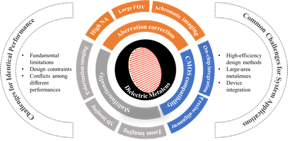
Despite the tremendous progress achieved so far, it is pointed out that several challenges should be addressed for the practical development of metalens-based imaging systems.
“High focusing efficiency is challenging for high-NA metalenses due to the fundamental phase discretization and diffraction constraints. The breakthrough broadband achromatic feature of metalens suffers from some fundamental constraints, design limitations, and fabrication challenges. Moreover, conflicts in metalens parameters and aberration correction capabilities should be manipulated. Regarding multifunctional metalenses, the overall efficiency is limited by not only the efficient component of power but also the crosstalk among the sub-units. Balancing the performances among different focal spots is also a tough task. In addition, common challenges are hindering further development of dielectric metalens-integrated systems, including limitations of conventional design methods, the scaling up of dielectric metalenses, and the approaches for integrated devices.”
“In turn, these challenges provide some possible future development directions of metalenses: (i) New strategies to break the conflicts among metalens performances. (ii) Multifunctional and reconfigurable metalenses that could replace complicated configurations of conventional optics. (iii) High-efficiency design methods for high-performance metalenses. (iv) High-efficiency fabrication and mass manufacturing methodologies for large-area metalenses.” the researchers added.
“By addressing the present challenges of metalenses and combining the non-local optics, we envision that metalens-based imaging systems would be increasingly compact and widely employed in future applications, ranging from camera modules for consumer photography and autonomous vehicles to wearable displays for AR/VR/MR and machine vision, to bioimaging and endoscopy, to signal processing and optical computation.” the researchers forecast.
####
For more information, please click here
Contacts:
Media Contact
Yaobiao Li
Light Publishing Center, Changchun Institute of Optics, Fine Mechanics And Physics, CAS
Office: 86-431-861-76851
Expert Contact
Meiyan Pan
Jihua Laboratory
Copyright © Light Publishing Center, Changchun Institute of Optics, Fine Mechanics And Physics, CAS
If you have a comment, please Contact us.Issuers of news releases, not 7th Wave, Inc. or Nanotechnology Now, are solely responsible for the accuracy of the content.
Bookmark:


| Related Links |
| Related News Press |
News and information
![]() Quantum computer improves AI predictions April 17th, 2026
Quantum computer improves AI predictions April 17th, 2026
![]() Flexible sensor gains sensitivity under pressure April 17th, 2026
Flexible sensor gains sensitivity under pressure April 17th, 2026
![]() A reusable chip for particulate matter sensing April 17th, 2026
A reusable chip for particulate matter sensing April 17th, 2026
![]() Detecting vibrational quantum beating in the predissociation dynamics of SF6 using time-resolved photoelectron spectroscopy April 17th, 2026
Detecting vibrational quantum beating in the predissociation dynamics of SF6 using time-resolved photoelectron spectroscopy April 17th, 2026
Imaging
![]() Simple algorithm paired with standard imaging tool could predict failure in lithium metal batteries August 8th, 2025
Simple algorithm paired with standard imaging tool could predict failure in lithium metal batteries August 8th, 2025
Possible Futures
![]() A fundamentally new therapeutic approach to cystic fibrosis: Nanobody repairs cellular defect April 17th, 2026
A fundamentally new therapeutic approach to cystic fibrosis: Nanobody repairs cellular defect April 17th, 2026
![]() UC Irvine physicists discover method to reverse ‘quantum scrambling’ : The work addresses the problem of information loss in quantum computing system April 17th, 2026
UC Irvine physicists discover method to reverse ‘quantum scrambling’ : The work addresses the problem of information loss in quantum computing system April 17th, 2026
Discoveries
![]() Quantum computer improves AI predictions April 17th, 2026
Quantum computer improves AI predictions April 17th, 2026
![]() Flexible sensor gains sensitivity under pressure April 17th, 2026
Flexible sensor gains sensitivity under pressure April 17th, 2026
![]() A reusable chip for particulate matter sensing April 17th, 2026
A reusable chip for particulate matter sensing April 17th, 2026
![]() Detecting vibrational quantum beating in the predissociation dynamics of SF6 using time-resolved photoelectron spectroscopy April 17th, 2026
Detecting vibrational quantum beating in the predissociation dynamics of SF6 using time-resolved photoelectron spectroscopy April 17th, 2026
Announcements
![]() A fundamentally new therapeutic approach to cystic fibrosis: Nanobody repairs cellular defect April 17th, 2026
A fundamentally new therapeutic approach to cystic fibrosis: Nanobody repairs cellular defect April 17th, 2026
![]() UC Irvine physicists discover method to reverse ‘quantum scrambling’ : The work addresses the problem of information loss in quantum computing system April 17th, 2026
UC Irvine physicists discover method to reverse ‘quantum scrambling’ : The work addresses the problem of information loss in quantum computing system April 17th, 2026
Interviews/Book Reviews/Essays/Reports/Podcasts/Journals/White papers/Posters
![]() A fundamentally new therapeutic approach to cystic fibrosis: Nanobody repairs cellular defect April 17th, 2026
A fundamentally new therapeutic approach to cystic fibrosis: Nanobody repairs cellular defect April 17th, 2026
![]() UC Irvine physicists discover method to reverse ‘quantum scrambling’ : The work addresses the problem of information loss in quantum computing system April 17th, 2026
UC Irvine physicists discover method to reverse ‘quantum scrambling’ : The work addresses the problem of information loss in quantum computing system April 17th, 2026
Automotive/Transportation
![]() Decoding hydrogen‑bond network of electrolyte for cryogenic durable aqueous zinc‑ion batteries January 30th, 2026
Decoding hydrogen‑bond network of electrolyte for cryogenic durable aqueous zinc‑ion batteries January 30th, 2026
![]() Sensors innovations for smart lithium-based batteries: advancements, opportunities, and potential challenges August 8th, 2025
Sensors innovations for smart lithium-based batteries: advancements, opportunities, and potential challenges August 8th, 2025
![]() Simple algorithm paired with standard imaging tool could predict failure in lithium metal batteries August 8th, 2025
Simple algorithm paired with standard imaging tool could predict failure in lithium metal batteries August 8th, 2025
|
|
||
|
|
||
| The latest news from around the world, FREE | ||
|
|
||
|
|
||
| Premium Products | ||
|
|
||
|
Only the news you want to read!
Learn More |
||
|
|
||
|
Full-service, expert consulting
Learn More |
||
|
|
||