Home > Press > Novel Flexible Terahertz Camera Can Inspect Objects with Diverse Shapes
 |
Abstract:
Published: February 16, 2021
Scientists at Tokyo Institute of Technology (Tokyo Tech) and RIKEN have developed a flexible, free-standing, and versatile terahertz (THz) camera patch. This novel camera overcomes the limitations of the conventional THz cameras that are bulky and rigid. With its high sensitivity, adaptability, and ease of filming irregularly shaped objects, it is a potential tool for effective quality control of complex devices.
Novel Flexible Terahertz Camera Can Inspect Objects with Diverse Shapes
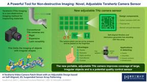
Tokyo, Japan | Posted on February 17th, 2021In today's digital age, the use of "Internet-of-things" (devices embedded with softwares and sensors) has become widespread. These devices include wireless equipment, autonomous machinery, wearable sensors, and security systems. With their intricate structures and properties stems the need to scrutinize them closely to assess their safety and utility and rule out any potential defects. But, at the same time, damage to the device during inspection must be avoided.
Terahertz (THz) imaging, based on radiation with frequencies between 0.1 and 10 THz, is one such non-destructive method that is rapidly gaining popularity owing to its high penetration, resolution, and sensitivity. Conventional THz cameras, however, are bulky and rigid, thereby limiting their potential in imaging uneven surfaces. Moreover, their high cost and lack of versatility in sensor configurations make them a rather impractical alternative, calling for more adaptable sensors.
To this end, a team of researchers from the Tokyo Tech, led by Associate Professor Yukio Kawano, have now addressed this gap by designing a flexible and free standing THz sensor array that can be used to image blind ends of irregularly shaped objects.
Ecstatic about their findings published in Advanced Functional Materials, Dr. Kawano states, "Given the diversity in shapes, structures, and sizes of test objects, the camera design and sensor must be adapted to conform to different configurations. In our study, we have developed a simple and cost-effective fabrication method for generating THz cameras with adaptable shapes."
The scientists knew that the material used in such sensors must have good absorption in the THz spectrum along with a high efficiency of converting emissions into detectable electric signals. For this reason, they selected carbon nanotube (CNT) films, which also possess good mechanical strength and flexibility. They passed the CNT solution through a polyimide film with laser induced slits and a membrane filter using a vacuum. Upon drying, the CNT solution remained as a free standing suspended structure between the layers of the patterned polyimide film. Further, they developed a simple fabrication process based on the self-assembly of CNT film array and its ability to from electrodes at both ends. For this, they evaporated metal electrodes over the patterned polyimide film. Together, these processes generated a THz camera patch sheet with multiple cameras. Interestingly, the structure of the suspended CNT film could be modified by altering the filtering conditions and thus the frictional force, making the process customizable.
Moreover, the patch sheet could be cut with scissors into smaller portable and wearable sensors that can be attached to the surface of the test object for better coverage. The researchers were able to demonstrate its industrial applications by detecting and visualizing cracks, impurities and uneven coating of polymers in a resin and by detecting sludge within a bent pipe, thus underscoring the potential of the camera in quality control operations.
Highlighting the applications of their design, Dr. Kawano remarks, "Our patch camera can be easily set up for imaging of large and unmovable objects. The unique 2D THz camera patch can ease restrictions pertaining to the shapes and locations of objects, contributing significantly to non-destructive monitoring sensor networks."
####
For more information, please click here
Contacts:
Corresponding author's email:
Further Information
Associate Professor Yukio Kawano
Institute of Innovative Research,
Tokyo Institute of Technology
Copyright © Tokyo Institute of Technology
If you have a comment, please Contact us.Issuers of news releases, not 7th Wave, Inc. or Nanotechnology Now, are solely responsible for the accuracy of the content.
Bookmark:


| Related Links |
| Related News Press |
News and information
![]() Simulating magnetization in a Heisenberg quantum spin chain April 5th, 2024
Simulating magnetization in a Heisenberg quantum spin chain April 5th, 2024
![]() NRL charters Navy�s quantum inertial navigation path to reduce drift April 5th, 2024
NRL charters Navy�s quantum inertial navigation path to reduce drift April 5th, 2024
![]() Discovery points path to flash-like memory for storing qubits: Rice find could hasten development of nonvolatile quantum memory April 5th, 2024
Discovery points path to flash-like memory for storing qubits: Rice find could hasten development of nonvolatile quantum memory April 5th, 2024
Imaging
![]() Nanoscale CL thermometry with lanthanide-doped heavy-metal oxide in TEM March 8th, 2024
Nanoscale CL thermometry with lanthanide-doped heavy-metal oxide in TEM March 8th, 2024
![]() The USTC realizes In situ electron paramagnetic resonance spectroscopy using single nanodiamond sensors November 3rd, 2023
The USTC realizes In situ electron paramagnetic resonance spectroscopy using single nanodiamond sensors November 3rd, 2023
![]() Observation of left and right at nanoscale with optical force October 6th, 2023
Observation of left and right at nanoscale with optical force October 6th, 2023
Possible Futures
![]() Discovery points path to flash-like memory for storing qubits: Rice find could hasten development of nonvolatile quantum memory April 5th, 2024
Discovery points path to flash-like memory for storing qubits: Rice find could hasten development of nonvolatile quantum memory April 5th, 2024
![]() With VECSELs towards the quantum internet Fraunhofer: IAF achieves record output power with VECSEL for quantum frequency converters April 5th, 2024
With VECSELs towards the quantum internet Fraunhofer: IAF achieves record output power with VECSEL for quantum frequency converters April 5th, 2024
Sensors
Discoveries
![]() Chemical reactions can scramble quantum information as well as black holes April 5th, 2024
Chemical reactions can scramble quantum information as well as black holes April 5th, 2024
![]() New micromaterial releases nanoparticles that selectively destroy cancer cells April 5th, 2024
New micromaterial releases nanoparticles that selectively destroy cancer cells April 5th, 2024
![]() Utilizing palladium for addressing contact issues of buried oxide thin film transistors April 5th, 2024
Utilizing palladium for addressing contact issues of buried oxide thin film transistors April 5th, 2024
Announcements
![]() NRL charters Navy�s quantum inertial navigation path to reduce drift April 5th, 2024
NRL charters Navy�s quantum inertial navigation path to reduce drift April 5th, 2024
![]() Discovery points path to flash-like memory for storing qubits: Rice find could hasten development of nonvolatile quantum memory April 5th, 2024
Discovery points path to flash-like memory for storing qubits: Rice find could hasten development of nonvolatile quantum memory April 5th, 2024
Interviews/Book Reviews/Essays/Reports/Podcasts/Journals/White papers/Posters
![]() Simulating magnetization in a Heisenberg quantum spin chain April 5th, 2024
Simulating magnetization in a Heisenberg quantum spin chain April 5th, 2024
![]() Discovery points path to flash-like memory for storing qubits: Rice find could hasten development of nonvolatile quantum memory April 5th, 2024
Discovery points path to flash-like memory for storing qubits: Rice find could hasten development of nonvolatile quantum memory April 5th, 2024
Tools
![]() Ferroelectrically modulate the Fermi level of graphene oxide to enhance SERS response November 3rd, 2023
Ferroelectrically modulate the Fermi level of graphene oxide to enhance SERS response November 3rd, 2023
![]() The USTC realizes In situ electron paramagnetic resonance spectroscopy using single nanodiamond sensors November 3rd, 2023
The USTC realizes In situ electron paramagnetic resonance spectroscopy using single nanodiamond sensors November 3rd, 2023
|
|
||
|
|
||
| The latest news from around the world, FREE | ||
|
|
||
|
|
||
| Premium Products | ||
|
|
||
|
Only the news you want to read!
Learn More |
||
|
|
||
|
Full-service, expert consulting
Learn More |
||
|
|
||