Home > Press > Machine learning helps improving photonic applications
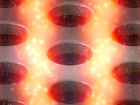 |
| The computer simulation shows how the electromagnetic field is distributed in the silicon layer with hole pattern after excitation with a laser. Here, stripes with local field maxima are formed, so that quantum dots shine particularly strongly. CREDIT Carlo Barth/HZB |
Abstract:
Nanostructures can increase the sensitivity of optical sensors enormously - provided that the geometry meets certain conditions and matches the wavelength of the incident light. This is because the electromagnetic field of light can be greatly amplified or reduced by the local nanostructure. The HZB Young Investigator Group "Nano-SIPPE" headed by Prof. Christiane Becker is working to develop these kinds of nanostructures. Computer simulations are an important tool for this. Dr. Carlo Barth from the Nano-SIPPE team has now identified the most important patterns of field distribution in a nanostructure using machine learning, and has thereby explained the experimental findings very well for the first time.
Machine learning helps improving photonic applications
Berlin, Germany | Posted on September 28th, 2018
Quantum dots on nanostructures
The photonic nanostructures examined in this paper consist of a silicon layer with a regular hole pattern coated with what are referred to as quantum dots made of lead sulphide. Excited with a laser, the quantum dots close to local field amplifications emit much more light than on an unordered surface. This makes it possible to empirically demonstrate how the laser light interacts with the nanostructure.
Ten different patterns discovered by machine learning
In order to systematically record what happens when individual parameters of the nanostructure change, Barth calculates the three-dimensional electric field distribution for each parameter set using software developed at the Zuse Institute Berlin. Barth then had these enormous amounts of data analyzed by other computer programs based on machine learning. "The computer has searched through the approximately 45,000 data records and grouped them into about ten different patterns", he explains. Finally, Barth and Becker succeeded in identifying three basic patterns among them in which the fields are amplified in various specific areas of the nanoholes.
Outlook: Detection of single molecules, e.g. cancer markers
This allows photonic crystal membranes based on excitation amplification to be optimised for virtually any application. This is because some biomolecules accumulate preferentially along the hole edges, for example, while others prefer the plateaus between the holes, depending on the application. With the correct geometry and the right excitation by light, the maximum electric field amplification can be generated exactly at the attachment sites of the desired molecules. This would increase the sensitivity of optical sensors for cancer markers to the level of individual molecules, for example.
###
The software used as well as the data can be downloaded free.
####
For more information, please click here
Contacts:
Antonia Roetger
Copyright © Helmholtz-Zentrum Berlin f�r Materialien und Energie
If you have a comment, please Contact us.Issuers of news releases, not 7th Wave, Inc. or Nanotechnology Now, are solely responsible for the accuracy of the content.
Bookmark:


| Related Links |
| Related News Press |
News and information
![]() Simulating magnetization in a Heisenberg quantum spin chain April 5th, 2024
Simulating magnetization in a Heisenberg quantum spin chain April 5th, 2024
![]() NRL charters Navy�s quantum inertial navigation path to reduce drift April 5th, 2024
NRL charters Navy�s quantum inertial navigation path to reduce drift April 5th, 2024
![]() Discovery points path to flash-like memory for storing qubits: Rice find could hasten development of nonvolatile quantum memory April 5th, 2024
Discovery points path to flash-like memory for storing qubits: Rice find could hasten development of nonvolatile quantum memory April 5th, 2024
Software
![]() Visualizing nanoscale structures in real time: Open-source software enables researchers to see materials in 3D while they're still on the electron microscope August 19th, 2022
Visualizing nanoscale structures in real time: Open-source software enables researchers to see materials in 3D while they're still on the electron microscope August 19th, 2022
![]() Luisier wins SNSF Advanced Grant to develop simulation tools for nanoscale devices July 8th, 2022
Luisier wins SNSF Advanced Grant to develop simulation tools for nanoscale devices July 8th, 2022
![]() Oxford Instruments� Atomfab� system is production-qualified at a market-leading GaN power electronics device manufacturer December 17th, 2021
Oxford Instruments� Atomfab� system is production-qualified at a market-leading GaN power electronics device manufacturer December 17th, 2021
Possible Futures
![]() Discovery points path to flash-like memory for storing qubits: Rice find could hasten development of nonvolatile quantum memory April 5th, 2024
Discovery points path to flash-like memory for storing qubits: Rice find could hasten development of nonvolatile quantum memory April 5th, 2024
![]() With VECSELs towards the quantum internet Fraunhofer: IAF achieves record output power with VECSEL for quantum frequency converters April 5th, 2024
With VECSELs towards the quantum internet Fraunhofer: IAF achieves record output power with VECSEL for quantum frequency converters April 5th, 2024
Chip Technology
![]() Discovery points path to flash-like memory for storing qubits: Rice find could hasten development of nonvolatile quantum memory April 5th, 2024
Discovery points path to flash-like memory for storing qubits: Rice find could hasten development of nonvolatile quantum memory April 5th, 2024
![]() Utilizing palladium for addressing contact issues of buried oxide thin film transistors April 5th, 2024
Utilizing palladium for addressing contact issues of buried oxide thin film transistors April 5th, 2024
![]() HKUST researchers develop new integration technique for efficient coupling of III-V and silicon February 16th, 2024
HKUST researchers develop new integration technique for efficient coupling of III-V and silicon February 16th, 2024
Optical computing/Photonic computing
![]() With VECSELs towards the quantum internet Fraunhofer: IAF achieves record output power with VECSEL for quantum frequency converters April 5th, 2024
With VECSELs towards the quantum internet Fraunhofer: IAF achieves record output power with VECSEL for quantum frequency converters April 5th, 2024
![]() Chemical reactions can scramble quantum information as well as black holes April 5th, 2024
Chemical reactions can scramble quantum information as well as black holes April 5th, 2024
![]() Optically trapped quantum droplets of light can bind together to form macroscopic complexes March 8th, 2024
Optically trapped quantum droplets of light can bind together to form macroscopic complexes March 8th, 2024
![]() HKUST researchers develop new integration technique for efficient coupling of III-V and silicon February 16th, 2024
HKUST researchers develop new integration technique for efficient coupling of III-V and silicon February 16th, 2024
Nanoelectronics
![]() Interdisciplinary: Rice team tackles the future of semiconductors Multiferroics could be the key to ultralow-energy computing October 6th, 2023
Interdisciplinary: Rice team tackles the future of semiconductors Multiferroics could be the key to ultralow-energy computing October 6th, 2023
![]() Key element for a scalable quantum computer: Physicists from Forschungszentrum J�lich and RWTH Aachen University demonstrate electron transport on a quantum chip September 23rd, 2022
Key element for a scalable quantum computer: Physicists from Forschungszentrum J�lich and RWTH Aachen University demonstrate electron transport on a quantum chip September 23rd, 2022
![]() Reduced power consumption in semiconductor devices September 23rd, 2022
Reduced power consumption in semiconductor devices September 23rd, 2022
![]() Atomic level deposition to extend Moore�s law and beyond July 15th, 2022
Atomic level deposition to extend Moore�s law and beyond July 15th, 2022
Discoveries
![]() Chemical reactions can scramble quantum information as well as black holes April 5th, 2024
Chemical reactions can scramble quantum information as well as black holes April 5th, 2024
![]() New micromaterial releases nanoparticles that selectively destroy cancer cells April 5th, 2024
New micromaterial releases nanoparticles that selectively destroy cancer cells April 5th, 2024
![]() Utilizing palladium for addressing contact issues of buried oxide thin film transistors April 5th, 2024
Utilizing palladium for addressing contact issues of buried oxide thin film transistors April 5th, 2024
Announcements
![]() NRL charters Navy�s quantum inertial navigation path to reduce drift April 5th, 2024
NRL charters Navy�s quantum inertial navigation path to reduce drift April 5th, 2024
![]() Discovery points path to flash-like memory for storing qubits: Rice find could hasten development of nonvolatile quantum memory April 5th, 2024
Discovery points path to flash-like memory for storing qubits: Rice find could hasten development of nonvolatile quantum memory April 5th, 2024
Interviews/Book Reviews/Essays/Reports/Podcasts/Journals/White papers/Posters
![]() Simulating magnetization in a Heisenberg quantum spin chain April 5th, 2024
Simulating magnetization in a Heisenberg quantum spin chain April 5th, 2024
![]() Discovery points path to flash-like memory for storing qubits: Rice find could hasten development of nonvolatile quantum memory April 5th, 2024
Discovery points path to flash-like memory for storing qubits: Rice find could hasten development of nonvolatile quantum memory April 5th, 2024
Quantum Dots/Rods
![]() A new kind of magnetism November 17th, 2023
A new kind of magnetism November 17th, 2023
![]() IOP Publishing celebrates World Quantum Day with the announcement of a special quantum collection and the winners of two prestigious quantum awards April 14th, 2023
IOP Publishing celebrates World Quantum Day with the announcement of a special quantum collection and the winners of two prestigious quantum awards April 14th, 2023
![]() Qubits on strong stimulants: Researchers find ways to improve the storage time of quantum information in a spin rich material January 27th, 2023
Qubits on strong stimulants: Researchers find ways to improve the storage time of quantum information in a spin rich material January 27th, 2023
![]() NIST�s grid of quantum islands could reveal secrets for powerful technologies November 18th, 2022
NIST�s grid of quantum islands could reveal secrets for powerful technologies November 18th, 2022
Photonics/Optics/Lasers
![]() With VECSELs towards the quantum internet Fraunhofer: IAF achieves record output power with VECSEL for quantum frequency converters April 5th, 2024
With VECSELs towards the quantum internet Fraunhofer: IAF achieves record output power with VECSEL for quantum frequency converters April 5th, 2024
![]() Nanoscale CL thermometry with lanthanide-doped heavy-metal oxide in TEM March 8th, 2024
Nanoscale CL thermometry with lanthanide-doped heavy-metal oxide in TEM March 8th, 2024
![]() Optically trapped quantum droplets of light can bind together to form macroscopic complexes March 8th, 2024
Optically trapped quantum droplets of light can bind together to form macroscopic complexes March 8th, 2024
![]() HKUST researchers develop new integration technique for efficient coupling of III-V and silicon February 16th, 2024
HKUST researchers develop new integration technique for efficient coupling of III-V and silicon February 16th, 2024
|
|
||
|
|
||
| The latest news from around the world, FREE | ||
|
|
||
|
|
||
| Premium Products | ||
|
|
||
|
Only the news you want to read!
Learn More |
||
|
|
||
|
Full-service, expert consulting
Learn More |
||
|
|
||