Home > Press > Leti & CMP Announce World’s First Multi-Project-Wafer Service with Integrated Silicon OxRAM: Oxide-Based Resistive Ram Memory Platform Development for Backend Memories To Offer Non-Volatility Associated with Embedded Designs
 |
Abstract:
Leti, a research institute at CEA Tech, and CMP, a service organization that provides prototyping and low-volume production of ICs and MEMS, today announced the integrated-circuit industry’s first multi-project-wafer (MPW) process for fabricating emerging non-volatile memory OxRAM devices on a 200mm foundry base-wafer platform.
Leti & CMP Announce World’s First Multi-Project-Wafer Service with Integrated Silicon OxRAM: Oxide-Based Resistive Ram Memory Platform Development for Backend Memories To Offer Non-Volatility Associated with Embedded Designs
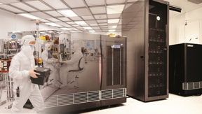
Grenoble, France | Posted on August 2nd, 2018Available on Leti’s 200mm CMOS line, the MPW service provides a comprehensive, very low-cost way to explore techniques designed to achieve miniaturized, high-density components. Including Leti’s Memory Advanced Demonstrator (MAD) future mask set with disruptive OxRAM (oxide-based resistive RAM) technology, Leti’s integrated silicon memory platform is developed for backend memories and non-volatility associated with embedded designs. The new technology platform will be based on HfO2/Ti (titanium-doped hafnium oxide) active layers.
Emerging OxRAM non-volatile memory is one of the promising technologies to be implemented for classical embedded memory applications on advanced nodes like micro-controllers or secure products, as well as for AI accelerators and neuromorphic computing.
Leti’s MAD platform is dedicated to advanced non-volatile memories, bringing both versatility and robustness for material and interface assessment, and allowing in-depth exploration of memory performance from technology and design perspectives.
The full platform’s highlights:
• 200mm STMicroelectronics HCMOS9A base wafers in 130nm node
• All routing is made on ST base wafers from M1 to M4 (included)
• Leti’s OxRAM memory module is fabricated on top
• One level of interconnect (i.e. M5) plus pads are fabricated in Leti’s cleanroom.
“Leti has developed during the past 20 years deep expertise in non-volatile memory (NVM) devices covering flash evolutive solutions and disruptive technologies,” said Etienne Nowak, head of the Leti’s Advanced Memory Lab. “This MPW capability, combined with our Memory Advanced Demonstrator platform, is based on a broad tool box that enables customized research with our partners, and provides a benchmark between different NVM solutions.”
The MPW service with integrated silicon OxRAM addresses all the key steps of advanced memory development. These include material engineering and analysis, developing critical memory modules, evaluation of memory cells coupled with electrical tests, modeling and innovative design techniques to comply with circuit design opportunities and constraints. This technology offer comes with a design kit, including layout, verification and simulation capabilities. Libraries are provided with a comprehensive list of active and passive electro-optical components. The design kit environment is compatible with all offers through CMP.
Providing access to a non-volatile memory process from Leti is a major achievement in development work at CMP. Since 2003, the organization has participated in national and European projects for developing access to NVM technologies (Mag-SPICE, Calomag, Cilomag, Spin, and Dipmem). With this new offer in place, the CMP users’ community can have the benefits and advantages of using this process through this close collaboration between CMP and Leti.
“CMP has a long experience providing smaller organizations with access to advanced manufacturing technologies, and there is very strong interest in the CMP community in designing and prototyping ICs using this process,” said Jean-Christophe Crébier, director of CMP. “It is an opportunity for many universities, start-ups and SMEs in France, Europe, North America and Asia to take advantage of this new technology and MPW service.”
About Flash Memory Summit
Flash Memory Summit, produced by Conference ConCepts, showcases the mainstream applications, key technologies and leading vendors that are driving the multi-billion dollar non-volatile memory and SSD markets. Now in its 13th year, FMS is the world’s largest event featuring the trends, innovations and influencers driving the adoption of Flash Memory in demanding enterprise storage applications, as well as in smartphones, tablets, and mobile and embedded systems.
####
About Leti
eti, a technology research institute at CEA Tech, is a global leader in miniaturization technologies enabling smart, energy-efficient and secure solutions for industry. Founded in 1967, Leti pioneers micro-& nanotechnologies, tailoring differentiating applicative solutions for global companies, SMEs and startups. Leti tackles critical challenges in healthcare, energy and digital migration. From sensors to data processing and computing solutions, Leti’s multidisciplinary teams deliver solid expertise, leveraging world-class pre-industrialization facilities. With a staff of more than 1,900, a portfolio of 2,700 patents, 91,500 sq. ft. of cleanroom space and a clear IP policy, the institute is based in Grenoble, France, and has offices in Silicon Valley and Tokyo. Leti has launched 60 startups and is a member of the Carnot Institutes network. Follow us on www.leti-cea.com and @CEA_Leti.
CEA Tech is the technology research branch of the French Alternative Energies and Atomic Energy Commission (CEA), a key player in innovative R&D, defence & security, nuclear energy, technological research for industry and fundamental science. CEA was named by Thomson Reuters as the second most innovative research organization in the world in 2017. CEA Tech leverages a unique innovation-driven culture and unrivalled expertise to develop and disseminate new technologies for industry, helping to create high-end products and provide a competitive edge.
About CMP
CMP, Circuits Multi-Projets®, is a service organization in ICs, Si photonics, Smart Power and MEMS for prototyping and low volume production. CMP enables prototypes fabrication on industrial processes at very attractive costs and offers great technical expertise in providing MPW and related services for Universities, Research Laboratories and Industrial companies’ prototyping. Chips are normally untested and delivered packaged or not. Advanced industrial technologies are made available in CMOS, SiGe BiCMOS, HV-CMOS, SOI, BCD, Si-Photonics, MEMS, 3D-IC, etc. Since 1981, more than 600 Institutions from 70 countries have been served, more than 7,900 projects have been prototyped through 1,000 runs, and 72 different technologies have been interfaced. For more information, visit: https://mycmp.fr
For more information, please click here
Contacts:
Leti
Etienne Nowak, (33) 4 38 78 09 88
Agency
Sarah-Lyle Dampoux
+33 6 74 93 23 47
CMP - Circuits Multi-Projets®
Jean-Christophe Crébier, (33) 4 76 57 46 15
Copyright © Leti
If you have a comment, please Contact us.Issuers of news releases, not 7th Wave, Inc. or Nanotechnology Now, are solely responsible for the accuracy of the content.
Bookmark:


| Related News Press |
News and information
![]() Simulating magnetization in a Heisenberg quantum spin chain April 5th, 2024
Simulating magnetization in a Heisenberg quantum spin chain April 5th, 2024
![]() NRL charters Navy’s quantum inertial navigation path to reduce drift April 5th, 2024
NRL charters Navy’s quantum inertial navigation path to reduce drift April 5th, 2024
![]() Discovery points path to flash-like memory for storing qubits: Rice find could hasten development of nonvolatile quantum memory April 5th, 2024
Discovery points path to flash-like memory for storing qubits: Rice find could hasten development of nonvolatile quantum memory April 5th, 2024
Possible Futures
![]() Discovery points path to flash-like memory for storing qubits: Rice find could hasten development of nonvolatile quantum memory April 5th, 2024
Discovery points path to flash-like memory for storing qubits: Rice find could hasten development of nonvolatile quantum memory April 5th, 2024
![]() With VECSELs towards the quantum internet Fraunhofer: IAF achieves record output power with VECSEL for quantum frequency converters April 5th, 2024
With VECSELs towards the quantum internet Fraunhofer: IAF achieves record output power with VECSEL for quantum frequency converters April 5th, 2024
Chip Technology
![]() Discovery points path to flash-like memory for storing qubits: Rice find could hasten development of nonvolatile quantum memory April 5th, 2024
Discovery points path to flash-like memory for storing qubits: Rice find could hasten development of nonvolatile quantum memory April 5th, 2024
![]() Utilizing palladium for addressing contact issues of buried oxide thin film transistors April 5th, 2024
Utilizing palladium for addressing contact issues of buried oxide thin film transistors April 5th, 2024
![]() HKUST researchers develop new integration technique for efficient coupling of III-V and silicon February 16th, 2024
HKUST researchers develop new integration technique for efficient coupling of III-V and silicon February 16th, 2024
Memory Technology
![]() Utilizing palladium for addressing contact issues of buried oxide thin film transistors April 5th, 2024
Utilizing palladium for addressing contact issues of buried oxide thin film transistors April 5th, 2024
![]() Interdisciplinary: Rice team tackles the future of semiconductors Multiferroics could be the key to ultralow-energy computing October 6th, 2023
Interdisciplinary: Rice team tackles the future of semiconductors Multiferroics could be the key to ultralow-energy computing October 6th, 2023
![]() Researchers discover materials exhibiting huge magnetoresistance June 9th, 2023
Researchers discover materials exhibiting huge magnetoresistance June 9th, 2023
Nanoelectronics
![]() Interdisciplinary: Rice team tackles the future of semiconductors Multiferroics could be the key to ultralow-energy computing October 6th, 2023
Interdisciplinary: Rice team tackles the future of semiconductors Multiferroics could be the key to ultralow-energy computing October 6th, 2023
![]() Key element for a scalable quantum computer: Physicists from Forschungszentrum Jülich and RWTH Aachen University demonstrate electron transport on a quantum chip September 23rd, 2022
Key element for a scalable quantum computer: Physicists from Forschungszentrum Jülich and RWTH Aachen University demonstrate electron transport on a quantum chip September 23rd, 2022
![]() Reduced power consumption in semiconductor devices September 23rd, 2022
Reduced power consumption in semiconductor devices September 23rd, 2022
![]() Atomic level deposition to extend Moore’s law and beyond July 15th, 2022
Atomic level deposition to extend Moore’s law and beyond July 15th, 2022
Announcements
![]() NRL charters Navy’s quantum inertial navigation path to reduce drift April 5th, 2024
NRL charters Navy’s quantum inertial navigation path to reduce drift April 5th, 2024
![]() Discovery points path to flash-like memory for storing qubits: Rice find could hasten development of nonvolatile quantum memory April 5th, 2024
Discovery points path to flash-like memory for storing qubits: Rice find could hasten development of nonvolatile quantum memory April 5th, 2024
Artificial Intelligence
![]() Simulating magnetization in a Heisenberg quantum spin chain April 5th, 2024
Simulating magnetization in a Heisenberg quantum spin chain April 5th, 2024
![]() Researchers’ approach may protect quantum computers from attacks March 8th, 2024
Researchers’ approach may protect quantum computers from attacks March 8th, 2024
![]() New chip opens door to AI computing at light speed February 16th, 2024
New chip opens door to AI computing at light speed February 16th, 2024
![]() HKUST researchers develop new integration technique for efficient coupling of III-V and silicon February 16th, 2024
HKUST researchers develop new integration technique for efficient coupling of III-V and silicon February 16th, 2024
Events/Classes
![]() Researchers demonstrate co-propagation of quantum and classical signals: Study shows that quantum encryption can be implemented in existing fiber networks January 20th, 2023
Researchers demonstrate co-propagation of quantum and classical signals: Study shows that quantum encryption can be implemented in existing fiber networks January 20th, 2023
Alliances/Trade associations/Partnerships/Distributorships
![]() Chicago Quantum Exchange welcomes six new partners highlighting quantum technology solutions, from Chicago and beyond September 23rd, 2022
Chicago Quantum Exchange welcomes six new partners highlighting quantum technology solutions, from Chicago and beyond September 23rd, 2022
![]() University of Illinois Chicago joins Brookhaven Lab's Quantum Center June 10th, 2022
University of Illinois Chicago joins Brookhaven Lab's Quantum Center June 10th, 2022
|
|
||
|
|
||
| The latest news from around the world, FREE | ||
|
|
||
|
|
||
| Premium Products | ||
|
|
||
|
Only the news you want to read!
Learn More |
||
|
|
||
|
Full-service, expert consulting
Learn More |
||
|
|
||