Home > Press > Leti Presents Optical-Equipment Curving Technology that Improves Performance, Cuts Costs: ‘Disruptive Approach’ for Imaging Applications Presented in Paper At Photonics West and Demonstrated in Leti’s Booth
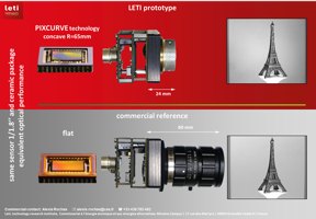 |
| Fig. 1: Leti’s prototype with PIXCURVE technology compared to a commercial reference: performance improves, while size, complexity and cost are reduced. |
Abstract:
Leti, a research institute at CEA Tech, has developed a new curving technology for optical sensors and micro-displays that improves performance, enhances field of view and compensates for aberrations in optical applications.
Leti Presents Optical-Equipment Curving Technology that Improves Performance, Cuts Costs: ‘Disruptive Approach’ for Imaging Applications Presented in Paper At Photonics West and Demonstrated in Leti’s Booth
San Francisco, CA | Posted on February 2nd, 2018The technology curves components such as CMOS imagers and charged-couple device (CCD) imagers for mobile phones, cameras, telescopes, medical-imaging tools and industrial-control equipment. Other uses include IR sensors for astronomy, defense, drones and micro-displays for automotive applications, augmented reality and virtual reality.
Leti’s fully functional prototype of this technology was presented today in the paper, “Curved Sensors for Compact High-Resolution Wide Field Designs: Prototype Demonstration and Optical Characterization”, at Photonics West 2018, in collaboration with LAM (Laboratoire d’Astrophysique de Marseille). Called PIXCURVE, it also is being demonstrated at Leti’s booth, 431, in the Moscone Center, where the conference is based.
“Curved sensor technology is a disruptive approach for imaging applications such as photography, videography, computer vision, surveillance and many other applications,” said Bertrand Chambion, one of the paper’s co-authors. “In recent years, we have seen very strong interest in curved electronics, particularly for opto-electronics systems whose performance improves, while size, complexity and cost are reduced.”
The demonstration is based on a 1/1.8’’ format, 1.3-million-pixel CMOS image sensor. The standard sensor structure consists of a 7.74 x 8.12 mm silicon die glued on a ceramic package. Electrical connections are wire bonded from the die to the package surface and, then, to the interconnection board. A glass cover is placed on top for mechanical protection.
Leti’s technology uses a grinding process to get the sensor below 100µm thick, which makes it mechanically flexible. It is then glued onto a curved substrate, which determines its final shape. A wire bonding process developed for electrical connections is used to prevent damages on the thinned dies. The radius of curvature is R=65mm. This prototype is compared to the equivalent commercial solution with flat sensor in Figure 1.
This process is compatible with any sensor size and with large-scale manufacturing processes.
####
About Leti
Leti, a technology research institute at CEA Tech, is a global leader in miniaturization technologies enabling smart, energy-efficient and secure solutions for industry. Founded in 1967, Leti pioneers micro-& nanotechnologies, tailoring differentiating applicative solutions for global companies, SMEs and startups. Leti tackles critical challenges in healthcare, energy and digital migration. From sensors to data processing and computing solutions, Leti’s multidisciplinary teams deliver solid expertise, leveraging world-class pre-industrialization facilities. With a staff of more than 1,900, a portfolio of 2,700 patents, 91,500 sq. ft. of cleanroom space and a clear IP policy, the institute is based in Grenoble, France, and has offices in Silicon Valley and Tokyo. Leti has launched 60 startups and is a member of the Carnot Institutes network. Follow us on www.leti-cea.com and @CEA_Leti.
CEA Tech is the technology research branch of the French Alternative Energies and Atomic Energy Commission (CEA), a key player in innovative R&D, defence & security, nuclear energy, technological research for industry and fundamental science, identified by Thomson Reuters as the second most innovative research organization in the world. CEA Tech leverages a unique innovation-driven culture and unrivalled expertise to develop and disseminate new technologies for industry, helping to create high-end products and provide a competitive edge.
For more information, please click here
Contacts:
Press Contact
Agency
+33 6 74 93 23 47
Copyright © Leti
If you have a comment, please Contact us.Issuers of news releases, not 7th Wave, Inc. or Nanotechnology Now, are solely responsible for the accuracy of the content.
Bookmark:


| Related News Press |
News and information
![]() Simulating magnetization in a Heisenberg quantum spin chain April 5th, 2024
Simulating magnetization in a Heisenberg quantum spin chain April 5th, 2024
![]() NRL charters Navy’s quantum inertial navigation path to reduce drift April 5th, 2024
NRL charters Navy’s quantum inertial navigation path to reduce drift April 5th, 2024
![]() Discovery points path to flash-like memory for storing qubits: Rice find could hasten development of nonvolatile quantum memory April 5th, 2024
Discovery points path to flash-like memory for storing qubits: Rice find could hasten development of nonvolatile quantum memory April 5th, 2024
Imaging
![]() Nanoscale CL thermometry with lanthanide-doped heavy-metal oxide in TEM March 8th, 2024
Nanoscale CL thermometry with lanthanide-doped heavy-metal oxide in TEM March 8th, 2024
![]() The USTC realizes In situ electron paramagnetic resonance spectroscopy using single nanodiamond sensors November 3rd, 2023
The USTC realizes In situ electron paramagnetic resonance spectroscopy using single nanodiamond sensors November 3rd, 2023
![]() Observation of left and right at nanoscale with optical force October 6th, 2023
Observation of left and right at nanoscale with optical force October 6th, 2023
Announcements
![]() NRL charters Navy’s quantum inertial navigation path to reduce drift April 5th, 2024
NRL charters Navy’s quantum inertial navigation path to reduce drift April 5th, 2024
![]() Discovery points path to flash-like memory for storing qubits: Rice find could hasten development of nonvolatile quantum memory April 5th, 2024
Discovery points path to flash-like memory for storing qubits: Rice find could hasten development of nonvolatile quantum memory April 5th, 2024
Events/Classes
![]() Researchers demonstrate co-propagation of quantum and classical signals: Study shows that quantum encryption can be implemented in existing fiber networks January 20th, 2023
Researchers demonstrate co-propagation of quantum and classical signals: Study shows that quantum encryption can be implemented in existing fiber networks January 20th, 2023
|
|
||
|
|
||
| The latest news from around the world, FREE | ||
|
|
||
|
|
||
| Premium Products | ||
|
|
||
|
Only the news you want to read!
Learn More |
||
|
|
||
|
Full-service, expert consulting
Learn More |
||
|
|
||