Home > Press > Columbia engineers create artificial graphene in a nanofabricated semiconductor structure: Researchers are the first to observe the electronic structure of graphene in an engineered semiconductor; finding could lead to progress in advanced optoelectronics and data processing
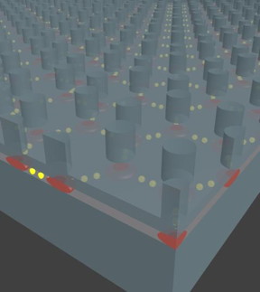 |
| Etched pillars define the positions of quantum dots (red puddles) arranged in an hexagonal lattice. When the spacing between the quantum dots is sufficiently small, electrons can move between them. CREDIT Diego Scarabelli/Columbia Engineering |
Abstract:
Researchers at Columbia Engineering, experts at manipulating matter at the nanoscale, have made an important breakthrough in physics and materials science, recently reported in Nature Nanotechnology. Working with colleagues from Princeton and Purdue Universities and Istituto Italiano di Tecnologia, the team has engineered "artificial graphene" by recreating, for the first time, the electronic structure of graphene in a semiconductor device.
Columbia engineers create artificial graphene in a nanofabricated semiconductor structure: Researchers are the first to observe the electronic structure of graphene in an engineered semiconductor; finding could lead to progress in advanced optoelectronics and data processing
New York, NY | Posted on December 13th, 2017"This milestone defines a new state-of-the-art in condensed matter science and nanofabrication," says Aron Pinczuk, professor of applied physics and physics at Columbia Engineering and senior author of the study. "While artificial graphene has been demonstrated in other systems such as optical, molecular, and photonic lattices, these platforms lack the versatility and potential offered by semiconductor processing technologies. Semiconductor artificial graphene devices could be platforms to explore new types of electronic switches, transistors with superior properties, and even, perhaps, new ways of storing information based on exotic quantum mechanical states."
The discovery of graphene in the early 2000s generated tremendous excitement in the physics community not only because it was the first real-world realization of a true two-dimensional material but also because the unique atomic arrangement of the carbon atoms in graphene provided a platform for testing new quantum phenomena that are difficult to observe in conventional materials systems. With its unusual electronic properties?its electrons can travel great distances before they are scattered?graphene is an outstanding conductor. These properties also display other unique characteristics that make electrons behave as if they are relativistic particles that move close to the speed of light, conferring upon them exotic properties that "regular," non-relativistic electrons do not have.
But graphene, a natural substance, comes in only one atomic arrangement: the positions of the atoms in the graphene lattice are fixed, and thus all experiments on graphene must adapt to those constraints. On the other hand, in artificial graphene the lattice can be engineered over a wide range of spacings and configurations, making it a holy grail of sorts for condensed matter researchers because it will have more versatile properties than the natural material.
"This is a rapidly expanding area of research, and we are uncovering new phenomena that couldn't be accessed before," says Shalom Wind, faculty member of the department of applied physics and applied mathematics and co-author of the study. "As we explore novel device concepts based on electrical control of artificial graphene, we can unlock the potential to expand frontiers in advanced optoelectronics and data processing."
"This work is really a major advance in artificial graphene. Since the first theoretical prediction that system with graphene-like electronic properties may be artificially created and tuned with patterned 2D electron gas, no one had succeeded, until the Columbia work, in directly observing these characteristics in engineered semiconductor nanostructures," says Steven G. Louie, professor of physics, University of California, Berkeley. "Previous work with molecules, atoms and photonic structures represent far less versatile and stable systems. The nanofabricated semiconductor structures open up tremendous opportunities for exploring exciting new science and practical applications."
The researchers used the tools of conventional chip technology to develop the artificial graphene in a standard semiconductor material, gallium arsenide. They designed a layered structure so that the electrons could move only within a very narrow layer, effectively creating a 2D sheet. They used nanolithography and etching to pattern the gallium arsenide: the patterning created a hexagonal lattice of sites in which the electrons were confined in the lateral direction. By placing these sites, which could be thought of as "artificial atoms," sufficiently close to one another (~ 50 nanometers apart), these artificial atoms could interact quantum mechanically, similar to the way atoms share their electrons in solids.
The team probed the electronic states of the artificial lattices by shining laser light on them and measuring the light that was scattered. The scattered light showed a loss of energy that corresponded to transitions in the electron energy from one state to another. When they mapped these transitions, the team found that they were approaching zero in a linear fashion around what is called the "Dirac point" where the electron density vanishes, a hallmark of graphene.
This artificial graphene has several advantages over natural graphene: for instance, researchers can design variations into the honeycomb lattice to modulate electronic behavior. And because the spacing between the quantum dots is much larger than the inter-atomic spacing in natural graphene, researchers can observe even more exotic quantum phenomena with the application of a magnetic field.
The discovery of new low-dimensional materials, such as graphene and other ultrathin, layered van der Waals films that exhibit exciting new physical phenomena that were previously inaccessible, laid the groundwork for this study. "What was really critical to our work was the impressive advancements in nanofabrication," Pinczuk notes. "These offer us an ever-increasing toolbox for creating a myriad of high-quality patterns at nanoscale dimensions. This is an exciting time to be a physicist working in our field."
####
About Columbia University School of Engineering and Applied Science
Columbia Engineering, based in New York City, is one of the top engineering schools in the U.S. and one of the oldest in the nation. Also known as The Fu Foundation School of Engineering and Applied Science, the School expands knowledge and advances technology through the pioneering research of its more than 200 faculty, while educating undergraduate and graduate students in a collaborative environment to become leaders informed by a firm foundation in engineering. The School's faculty are at the center of the University's cross-disciplinary research, contributing to the Data Science Institute, Earth Institute, Zuckerman Mind Brain Behavior Institute, Precision Medicine Initiative, and the Columbia Nano Initiative. Guided by its strategic vision, "Columbia Engineering for Humanity," the School aims to translate ideas into innovations that foster a sustainable, healthy, secure, connected, and creative humanity.
Disclaimer
For more information, please click here
Contacts:
Holly Evarts
212-854-3206
Copyright © Columbia University School of Engineering and Applied Science
If you have a comment, please Contact us.Issuers of news releases, not 7th Wave, Inc. or Nanotechnology Now, are solely responsible for the accuracy of the content.
Bookmark:


| Related Links |
| Related News Press |
News and information
![]() Gene therapy relieves back pain, repairs damaged disc in mice: Study suggests nanocarriers loaded with DNA could replace opioids May 17th, 2024
Gene therapy relieves back pain, repairs damaged disc in mice: Study suggests nanocarriers loaded with DNA could replace opioids May 17th, 2024
![]() Oscillating paramagnetic Meissner effect and Berezinskii-Kosterlitz-Thouless transition in cuprate superconductor May 17th, 2024
Oscillating paramagnetic Meissner effect and Berezinskii-Kosterlitz-Thouless transition in cuprate superconductor May 17th, 2024
![]() What is "time" for quantum particles? Publication by TU Darmstadt researchers in renowned journal "Science Advances" May 17th, 2024
What is "time" for quantum particles? Publication by TU Darmstadt researchers in renowned journal "Science Advances" May 17th, 2024
Physics
![]() Finding quantum order in chaos May 17th, 2024
Finding quantum order in chaos May 17th, 2024
![]() What is "time" for quantum particles? Publication by TU Darmstadt researchers in renowned journal "Science Advances" May 17th, 2024
What is "time" for quantum particles? Publication by TU Darmstadt researchers in renowned journal "Science Advances" May 17th, 2024
![]() Chemical reactions can scramble quantum information as well as black holes April 5th, 2024
Chemical reactions can scramble quantum information as well as black holes April 5th, 2024
Quantum Physics
![]() Finding quantum order in chaos May 17th, 2024
Finding quantum order in chaos May 17th, 2024
![]() Discovery points path to flash-like memory for storing qubits: Rice find could hasten development of nonvolatile quantum memory April 5th, 2024
Discovery points path to flash-like memory for storing qubits: Rice find could hasten development of nonvolatile quantum memory April 5th, 2024
![]() With VECSELs towards the quantum internet Fraunhofer: IAF achieves record output power with VECSEL for quantum frequency converters April 5th, 2024
With VECSELs towards the quantum internet Fraunhofer: IAF achieves record output power with VECSEL for quantum frequency converters April 5th, 2024
2 Dimensional Materials
![]() Oscillating paramagnetic Meissner effect and Berezinskii-Kosterlitz-Thouless transition in cuprate superconductor May 17th, 2024
Oscillating paramagnetic Meissner effect and Berezinskii-Kosterlitz-Thouless transition in cuprate superconductor May 17th, 2024
![]() NRL discovers two-dimensional waveguides February 16th, 2024
NRL discovers two-dimensional waveguides February 16th, 2024
Magnetism/Magnons
![]() Simulating magnetization in a Heisenberg quantum spin chain April 5th, 2024
Simulating magnetization in a Heisenberg quantum spin chain April 5th, 2024
Graphene/ Graphite
![]() NRL discovers two-dimensional waveguides February 16th, 2024
NRL discovers two-dimensional waveguides February 16th, 2024
Nanofabrication
![]() New chip opens door to AI computing at light speed February 16th, 2024
New chip opens door to AI computing at light speed February 16th, 2024
Govt.-Legislation/Regulation/Funding/Policy
![]() Aston University researcher receives �1 million grant to revolutionize miniature optical devices May 17th, 2024
Aston University researcher receives �1 million grant to revolutionize miniature optical devices May 17th, 2024
![]() NRL charters Navy�s quantum inertial navigation path to reduce drift April 5th, 2024
NRL charters Navy�s quantum inertial navigation path to reduce drift April 5th, 2024
![]() Discovery points path to flash-like memory for storing qubits: Rice find could hasten development of nonvolatile quantum memory April 5th, 2024
Discovery points path to flash-like memory for storing qubits: Rice find could hasten development of nonvolatile quantum memory April 5th, 2024
Possible Futures
![]() Advances in priming B cell immunity against HIV pave the way to future HIV vaccines, shows quartet of new studies May 17th, 2024
Advances in priming B cell immunity against HIV pave the way to future HIV vaccines, shows quartet of new studies May 17th, 2024
![]() Aston University researcher receives �1 million grant to revolutionize miniature optical devices May 17th, 2024
Aston University researcher receives �1 million grant to revolutionize miniature optical devices May 17th, 2024
![]() Gene therapy relieves back pain, repairs damaged disc in mice: Study suggests nanocarriers loaded with DNA could replace opioids May 17th, 2024
Gene therapy relieves back pain, repairs damaged disc in mice: Study suggests nanocarriers loaded with DNA could replace opioids May 17th, 2024
Chip Technology
![]() Diamond glitter: A play of colors with artificial DNA crystals May 17th, 2024
Diamond glitter: A play of colors with artificial DNA crystals May 17th, 2024
![]() Oscillating paramagnetic Meissner effect and Berezinskii-Kosterlitz-Thouless transition in cuprate superconductor May 17th, 2024
Oscillating paramagnetic Meissner effect and Berezinskii-Kosterlitz-Thouless transition in cuprate superconductor May 17th, 2024
![]() Discovery points path to flash-like memory for storing qubits: Rice find could hasten development of nonvolatile quantum memory April 5th, 2024
Discovery points path to flash-like memory for storing qubits: Rice find could hasten development of nonvolatile quantum memory April 5th, 2024
![]() Utilizing palladium for addressing contact issues of buried oxide thin film transistors April 5th, 2024
Utilizing palladium for addressing contact issues of buried oxide thin film transistors April 5th, 2024
Nanoelectronics
![]() Interdisciplinary: Rice team tackles the future of semiconductors Multiferroics could be the key to ultralow-energy computing October 6th, 2023
Interdisciplinary: Rice team tackles the future of semiconductors Multiferroics could be the key to ultralow-energy computing October 6th, 2023
![]() Key element for a scalable quantum computer: Physicists from Forschungszentrum J�lich and RWTH Aachen University demonstrate electron transport on a quantum chip September 23rd, 2022
Key element for a scalable quantum computer: Physicists from Forschungszentrum J�lich and RWTH Aachen University demonstrate electron transport on a quantum chip September 23rd, 2022
![]() Reduced power consumption in semiconductor devices September 23rd, 2022
Reduced power consumption in semiconductor devices September 23rd, 2022
![]() Atomic level deposition to extend Moore�s law and beyond July 15th, 2022
Atomic level deposition to extend Moore�s law and beyond July 15th, 2022
Discoveries
![]() Diamond glitter: A play of colors with artificial DNA crystals May 17th, 2024
Diamond glitter: A play of colors with artificial DNA crystals May 17th, 2024
![]() Finding quantum order in chaos May 17th, 2024
Finding quantum order in chaos May 17th, 2024
![]() Advances in priming B cell immunity against HIV pave the way to future HIV vaccines, shows quartet of new studies May 17th, 2024
Advances in priming B cell immunity against HIV pave the way to future HIV vaccines, shows quartet of new studies May 17th, 2024
Announcements
![]() Diamond glitter: A play of colors with artificial DNA crystals May 17th, 2024
Diamond glitter: A play of colors with artificial DNA crystals May 17th, 2024
![]() Finding quantum order in chaos May 17th, 2024
Finding quantum order in chaos May 17th, 2024
![]() Oscillating paramagnetic Meissner effect and Berezinskii-Kosterlitz-Thouless transition in cuprate superconductor May 17th, 2024
Oscillating paramagnetic Meissner effect and Berezinskii-Kosterlitz-Thouless transition in cuprate superconductor May 17th, 2024
Grants/Sponsored Research/Awards/Scholarships/Gifts/Contests/Honors/Records
![]() Aston University researcher receives �1 million grant to revolutionize miniature optical devices May 17th, 2024
Aston University researcher receives �1 million grant to revolutionize miniature optical devices May 17th, 2024
![]() Discovery points path to flash-like memory for storing qubits: Rice find could hasten development of nonvolatile quantum memory April 5th, 2024
Discovery points path to flash-like memory for storing qubits: Rice find could hasten development of nonvolatile quantum memory April 5th, 2024
![]() Chemical reactions can scramble quantum information as well as black holes April 5th, 2024
Chemical reactions can scramble quantum information as well as black holes April 5th, 2024
Quantum nanoscience
![]() What is "time" for quantum particles? Publication by TU Darmstadt researchers in renowned journal "Science Advances" May 17th, 2024
What is "time" for quantum particles? Publication by TU Darmstadt researchers in renowned journal "Science Advances" May 17th, 2024
![]() Simulating magnetization in a Heisenberg quantum spin chain April 5th, 2024
Simulating magnetization in a Heisenberg quantum spin chain April 5th, 2024
![]() Optically trapped quantum droplets of light can bind together to form macroscopic complexes March 8th, 2024
Optically trapped quantum droplets of light can bind together to form macroscopic complexes March 8th, 2024
![]() Bridging light and electrons January 12th, 2024
Bridging light and electrons January 12th, 2024
|
|
||
|
|
||
| The latest news from around the world, FREE | ||
|
|
||
|
|
||
| Premium Products | ||
|
|
||
|
Only the news you want to read!
Learn More |
||
|
|
||
|
Full-service, expert consulting
Learn More |
||
|
|
||