Home > Press > Electrons in graphene behave like light, only better: Researchers discover that electrons mimic light in graphene, confirming a 2007 prediction – their finding may enable new low power electronics and lead to new experimental probes
 |
Abstract:
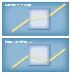
A team led by Cory Dean, assistant professor of physics at Columbia University, Avik Ghosh, professor of electrical and computer engineering at the University of Virginia, and James Hone, Wang Fong-Jen Professor of Mechanical Engineering at Columbia Engineering, has directly observed—for the first time—negative refraction for electrons passing across a boundary between two regions in a conducting material. First predicted in 2007, this effect has been difficult to confirm experimentally. The researchers were able to observe the effect in graphene, demonstrating that electrons in the atomically thin material behave like light rays, which can be manipulated by such optical devices as lenses and prisms. The findings, which are published in the September 30 edition of Science, could lead to the development of new types of electron switches, based on the principles of optics rather than electronics.
Electrons in graphene behave like light, only better: Researchers discover that electrons mimic light in graphene, confirming a 2007 prediction – their finding may enable new low power electronics and lead to new experimental probes
New York, NY | Posted on October 5th, 2016“The ability to manipulate electrons in a conducting material like light rays opens up entirely new ways of thinking about electronics,” says Dean. “For example, the switches that make up computer chips operate by turning the entire device on or off, and this consumes significant power. Using lensing to steer an electron ‘beam’ between electrodes could be dramatically more efficient, solving one of the critical bottlenecks to achieving faster and more energy efficient electronics.”
Dean adds, “These findings could also enable new experimental probes. For example, electron lensing could enable on-chip versions of an electron microscope, with the ability to perform atomic scale imageing and diagnostics. Other components inspired by optics, such as beam splitters and interferometers, could additionally enable new studies of the quantum nature of electrons in the solid state.”
While graphene has been widely explored for supporting high electron speed, it is notoriously hard to turn off the electrons without hurting their mobility. Ghosh says, “The natural follow-up is to see if we can achieve a strong current turn-off in graphene with multiple angled junctions. If that works to our satisfaction, we’ll have on our hands a low-power, ultra-high-speed switching device for both analog (RF) and digital (CMOS) electronics, potentially mitigating many of the challenges we face with the high energy cost and thermal budget of present day electronics.”
Light changes direction – or refracts - when passing from one material to another, a process that allows us to use lenses and prisms to focus and steer light. A quantity known as the index of refraction determines the degree of bending at the boundary, and is positive for conventional materials such as glass. However, through clever engineering, it is also possible to create optical “metamaterials” with a negative index, in which the angle of refraction is also negative. “This can have unusual and dramatic consequences,” Hone notes. “Optical metamaterials are enabling exotic and important new technologies such as super lenses, which can focus beyond the diffraction limit, and optical cloaks, which make objects invisible by bending light around them.”
Electrons travelling through very pure conductors can travel in straight lines like light rays, enabling optics-like phenomena to emerge. In materials, the electron density plays a similar role to the index of refraction, and electrons refract when they pass from a region of one density to another. Moreover, current carriers in materials can either behave like they are negatively charged (electrons) or positively charged (holes), depending on whether they inhabit the conduction or the valence band. In fact, boundaries between hole-type and electron-type conductors, known as p-n junctions (“p” positive, “n” negative), form the building blocks of electrical devices such as diodes and transistors.
“Unlike in optical materials”, says Hone, “where creating a negative index metamaterial is a significant engineering challenge, negative electron refraction occurs naturally in solid state materials at any p-n junction.”
The development of two-dimensional conducting layers in high-purity semiconductors such as GaAs (Gallium arsenide) in the 1980s and 1990s allowed researchers to first demonstrate electron optics including the effects of both refraction and lensing. However, in these materials, electrons travel without scattering only at very low temperatures, limiting technological applications. Furthermore, the presence of an energy gap between the conduction and valence band scatters electrons at interfaces and prevents observation of negative refraction in semiconductor p-n junctions. In this study, the researchers’ use of graphene, a 2D material with unsurpassed performance at room temperature and no energy gap, overcame both of these limitations.
The possibility of negative refraction at graphene p-n junctions was first proposed in 2007 by theorists working at both the University of Lancaster and Columbia University. However, observation of this effect requires extremely clean devices, such that the electrons can travel ballistically, without scattering, over long distances. Over the past decade, a multidisciplinary team at Columbia - including Hone and Dean, along with Kenneth Shepard, Lau Family Professor of Electrical Engineering and professor of biomedical engineering, Abhay Pasupathy, associate professor of physics, and Philip Kim, professor of physic at the time (now at Harvard) – has worked to develop new techniques to construct extremely clean graphene devices. This effort culminated in the 2013 demonstration of ballistic transport over a length scale in excess of 20 microns. Since then, they have been attempting to develop a Veselago lens, which focuses electrons to a single point using negative refraction. But they were unable to observe such an effect and found their results puzzling.
In 2015, a group at Pohang University of Science and Technology in South Korea reported the first evidence focusing in a Veselago-type device. However, the response was weak, appearing in the signal derivative. The Columbia team decided that to fully understand why the effect was so elusive, they needed to isolate and map the flow of electrons across the junction. They utilized a well-developed technique called “magnetic focusing” to inject electrons onto the p-n junction. By measuring transmission between electrodes on opposite sides of the junction as a function of carrier density they could map the trajectory of electrons on both sides of the p-n junction as the incident angle was changed by tuning the magnetic field.
Crucial to the Columbia effort was the theoretical support provided by Ghosh’s group at the University of Virginia, who developed detailed simulation techniques to model the Columbia team’s measured response. This involved calculating the flow of electrons in graphene under the various electric and magnetic fields, accounting for multiple bounces at edges, and quantum mechanical tunneling at the junction. The theoretical analysis also shed light on why it has been so difficult to measure the predicted Veselago lensing in a robust way, and the group is developing new multi-junction device architectures based on this study. Together the experimental data and theoretical simulation gave the researchers a visual map of the refraction, and enabled them to be the first to quantitatively confirm the relationship between the incident and refracted angles (known as Snell’s Law in optics), as well as confirmation of the magnitude of the transmitted intensity as a function of angle (known as the Fresnel coefficients in optics).
“In many ways, this intensity of transmission is a more crucial parameter,” says Ghosh, “since it determines the probability that electrons actually make it past the barrier, rather than just their refracted angles. The transmission ultimately determines many of the performance metrics for devices based on these effects, such as the on-off ratio in a switch, for example.”
The Science study was supported by Semiconductor Research Corporation’s NRI Center for Institute for Nanoelectronics Discovery and Exploration (INDEX). The collaboration was made possible through the support of the NRI program, which has brought together some of the country’s best groups in the study of 2D materials to focus on novel device architectures that may outperform conventional silicon-based technologies.
####
For more information, please click here
Contacts:
Holly Evarts
Director
Strategic Communications and Media Relations
Columbia Engineering
212-854-3206 (o)
347-453-7408 (c)
Elizabeth Thiel Mather
Director of Communications
University of Virginia
School of Engineering and Applied Science
434-924-1381 (o)
757-319-3664 (c)
Copyright © Columbia University School of Engineering and Applied Science
If you have a comment, please Contact us.Issuers of news releases, not 7th Wave, Inc. or Nanotechnology Now, are solely responsible for the accuracy of the content.
Bookmark:


| Related Links |
| Related News Press |
News and information
![]() Simulating magnetization in a Heisenberg quantum spin chain April 5th, 2024
Simulating magnetization in a Heisenberg quantum spin chain April 5th, 2024
![]() NRL charters Navy’s quantum inertial navigation path to reduce drift April 5th, 2024
NRL charters Navy’s quantum inertial navigation path to reduce drift April 5th, 2024
![]() Discovery points path to flash-like memory for storing qubits: Rice find could hasten development of nonvolatile quantum memory April 5th, 2024
Discovery points path to flash-like memory for storing qubits: Rice find could hasten development of nonvolatile quantum memory April 5th, 2024
2 Dimensional Materials
![]() NRL discovers two-dimensional waveguides February 16th, 2024
NRL discovers two-dimensional waveguides February 16th, 2024
Graphene/ Graphite
![]() NRL discovers two-dimensional waveguides February 16th, 2024
NRL discovers two-dimensional waveguides February 16th, 2024
Possible Futures
![]() Discovery points path to flash-like memory for storing qubits: Rice find could hasten development of nonvolatile quantum memory April 5th, 2024
Discovery points path to flash-like memory for storing qubits: Rice find could hasten development of nonvolatile quantum memory April 5th, 2024
![]() With VECSELs towards the quantum internet Fraunhofer: IAF achieves record output power with VECSEL for quantum frequency converters April 5th, 2024
With VECSELs towards the quantum internet Fraunhofer: IAF achieves record output power with VECSEL for quantum frequency converters April 5th, 2024
Chip Technology
![]() Discovery points path to flash-like memory for storing qubits: Rice find could hasten development of nonvolatile quantum memory April 5th, 2024
Discovery points path to flash-like memory for storing qubits: Rice find could hasten development of nonvolatile quantum memory April 5th, 2024
![]() Utilizing palladium for addressing contact issues of buried oxide thin film transistors April 5th, 2024
Utilizing palladium for addressing contact issues of buried oxide thin film transistors April 5th, 2024
![]() HKUST researchers develop new integration technique for efficient coupling of III-V and silicon February 16th, 2024
HKUST researchers develop new integration technique for efficient coupling of III-V and silicon February 16th, 2024
Nanoelectronics
![]() Interdisciplinary: Rice team tackles the future of semiconductors Multiferroics could be the key to ultralow-energy computing October 6th, 2023
Interdisciplinary: Rice team tackles the future of semiconductors Multiferroics could be the key to ultralow-energy computing October 6th, 2023
![]() Key element for a scalable quantum computer: Physicists from Forschungszentrum Jülich and RWTH Aachen University demonstrate electron transport on a quantum chip September 23rd, 2022
Key element for a scalable quantum computer: Physicists from Forschungszentrum Jülich and RWTH Aachen University demonstrate electron transport on a quantum chip September 23rd, 2022
![]() Reduced power consumption in semiconductor devices September 23rd, 2022
Reduced power consumption in semiconductor devices September 23rd, 2022
![]() Atomic level deposition to extend Moore’s law and beyond July 15th, 2022
Atomic level deposition to extend Moore’s law and beyond July 15th, 2022
Discoveries
![]() Chemical reactions can scramble quantum information as well as black holes April 5th, 2024
Chemical reactions can scramble quantum information as well as black holes April 5th, 2024
![]() New micromaterial releases nanoparticles that selectively destroy cancer cells April 5th, 2024
New micromaterial releases nanoparticles that selectively destroy cancer cells April 5th, 2024
![]() Utilizing palladium for addressing contact issues of buried oxide thin film transistors April 5th, 2024
Utilizing palladium for addressing contact issues of buried oxide thin film transistors April 5th, 2024
Announcements
![]() NRL charters Navy’s quantum inertial navigation path to reduce drift April 5th, 2024
NRL charters Navy’s quantum inertial navigation path to reduce drift April 5th, 2024
![]() Discovery points path to flash-like memory for storing qubits: Rice find could hasten development of nonvolatile quantum memory April 5th, 2024
Discovery points path to flash-like memory for storing qubits: Rice find could hasten development of nonvolatile quantum memory April 5th, 2024
Grants/Sponsored Research/Awards/Scholarships/Gifts/Contests/Honors/Records
![]() Discovery points path to flash-like memory for storing qubits: Rice find could hasten development of nonvolatile quantum memory April 5th, 2024
Discovery points path to flash-like memory for storing qubits: Rice find could hasten development of nonvolatile quantum memory April 5th, 2024
![]() Chemical reactions can scramble quantum information as well as black holes April 5th, 2024
Chemical reactions can scramble quantum information as well as black holes April 5th, 2024
Photonics/Optics/Lasers
![]() With VECSELs towards the quantum internet Fraunhofer: IAF achieves record output power with VECSEL for quantum frequency converters April 5th, 2024
With VECSELs towards the quantum internet Fraunhofer: IAF achieves record output power with VECSEL for quantum frequency converters April 5th, 2024
![]() Nanoscale CL thermometry with lanthanide-doped heavy-metal oxide in TEM March 8th, 2024
Nanoscale CL thermometry with lanthanide-doped heavy-metal oxide in TEM March 8th, 2024
![]() Optically trapped quantum droplets of light can bind together to form macroscopic complexes March 8th, 2024
Optically trapped quantum droplets of light can bind together to form macroscopic complexes March 8th, 2024
![]() HKUST researchers develop new integration technique for efficient coupling of III-V and silicon February 16th, 2024
HKUST researchers develop new integration technique for efficient coupling of III-V and silicon February 16th, 2024
|
|
||
|
|
||
| The latest news from around the world, FREE | ||
|
|
||
|
|
||
| Premium Products | ||
|
|
||
|
Only the news you want to read!
Learn More |
||
|
|
||
|
Full-service, expert consulting
Learn More |
||
|
|
||