Home > Press > Leti and EVG Launch INSPIRE, a Lithography Program Aimed At Demonstrating Benefits of Nano-imprint Technology
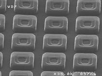 |
| CEA-Leti� Diffractive optical element realized by nanoimprint |
Abstract:
CEA-Leti and EV Group have launched a new program in nano-imprint lithography (NIL) called INSPIRE to demonstrate the benefits of the versatile, powerful nano-patterning technology and spread its use for applications beyond semiconductors.
Leti and EVG Launch INSPIRE, a Lithography Program Aimed At Demonstrating Benefits of Nano-imprint Technology
Grenoble, France and St Florian Am Inn, Austria | Posted on July 15th, 2015In addition to creating an industrial partnership to develop NIL process solutions, the INSPIRE program is designed to demonstrate the technology�s cost-of-ownership benefits for a wide range of application domains, such as photonics, plasmonics, lighting, photovoltaics, wafer-level optics and bio-technology.
Leti and EVG will jointly support the development of new applications from the feasibility-study stage to supporting the first manufacturing steps on EVG platforms and transferring integrated process solutions to their industrial partners, thus significantly lowering the entry barrier for adoption of NIL for manufacturing novel products.
In its effort to support high-volume manufacturing applications, EVG recently launched the HERCULES� NIL equipment platform, and the INSPIRE program�s activities will complement the company�s efforts within the framework of its NILPhotonicsTM competence center that was launched in December 2014.
�EVG is excited about the value that the partnership with Leti in the INSPIRE program will provide to industry,� said Markus Wimplinger, corporate technology development and IP director at EV Group. �After more than a decade of research and development activities, EVG has propelled NIL technology to a level of maturity that enables significant advantages for certain applications compared to traditional optical lithography.�
After launching its NIL technology-development program more than 10 years ago, Leti oriented the use of this technology mainly for photonics applications. In early 2014, the program was integrated in the Silicon Technologies Division to establish a NIL collaborative program.
�Leti and EVG have a long history of collaborating on ways to bring new technologies to market at reasonable costs for the benefits of our customers,� said Laurent Pain, patterning program manager in Leti�s Silicon Technologies Division. �Through INSPIRE, we will develop new ways for them to use this flexible, powerful nano-patterning technology to create new products for a wide range of applications.�
####
About CEA-Leti
As one of three advanced-research institutes within the CEA Technological Research Division, CEA Tech-Leti serves as a bridge between basic research and production of micro- and nanotechnologies that improve the lives of people around the world. It is committed to creating innovation and transferring it to industry. Backed by its portfolio of 2,800 patents, Leti partners with large industrials, SMEs and startups to tailor advanced solutions that strengthen their competitive positions. It has launched 54 startups. Its 8,500m� of new-generation cleanroom space feature 200mm and 300mm wafer processing of micro and nano solutions for applications ranging from space to smart devices. With a staff of more than 1,800, Leti is based in Grenoble, France, and has offices in Silicon Valley, Calif., and Tokyo. Follow us on www.leti.fr and @CEA_Leti.
About EVG (Austria)
EV Group (EVG) is a leading supplier of equipment and process solutions for the manufacture of semiconductors, microelectromechanical systems (MEMS), compound semiconductors, power devices and nanotechnology devices. Key products include wafer bonding, thin-wafer processing, lithography/nanoimprint lithography (NIL) and metrology equipment, as well as photoresist coaters, cleaners and inspection systems. Founded in 1980, EV Group services and supports an elaborate network of global customers and partners all over the world. More information about EVG is available at www.EVGroup.com
For more information, please click here
Contacts:
Leti Agency
+33 6 74 93 23 47
EV Group (EVG)
Marketing & Com
+43 7712 5311 0
Copyright © CEA-Leti
If you have a comment, please Contact us.Issuers of news releases, not 7th Wave, Inc. or Nanotechnology Now, are solely responsible for the accuracy of the content.
Bookmark:


| Related News Press |
News and information
![]() Simulating magnetization in a Heisenberg quantum spin chain April 5th, 2024
Simulating magnetization in a Heisenberg quantum spin chain April 5th, 2024
![]() NRL charters Navy�s quantum inertial navigation path to reduce drift April 5th, 2024
NRL charters Navy�s quantum inertial navigation path to reduce drift April 5th, 2024
![]() Discovery points path to flash-like memory for storing qubits: Rice find could hasten development of nonvolatile quantum memory April 5th, 2024
Discovery points path to flash-like memory for storing qubits: Rice find could hasten development of nonvolatile quantum memory April 5th, 2024
Chip Technology
![]() Discovery points path to flash-like memory for storing qubits: Rice find could hasten development of nonvolatile quantum memory April 5th, 2024
Discovery points path to flash-like memory for storing qubits: Rice find could hasten development of nonvolatile quantum memory April 5th, 2024
![]() Utilizing palladium for addressing contact issues of buried oxide thin film transistors April 5th, 2024
Utilizing palladium for addressing contact issues of buried oxide thin film transistors April 5th, 2024
![]() HKUST researchers develop new integration technique for efficient coupling of III-V and silicon February 16th, 2024
HKUST researchers develop new integration technique for efficient coupling of III-V and silicon February 16th, 2024
Nanoelectronics
![]() Interdisciplinary: Rice team tackles the future of semiconductors Multiferroics could be the key to ultralow-energy computing October 6th, 2023
Interdisciplinary: Rice team tackles the future of semiconductors Multiferroics could be the key to ultralow-energy computing October 6th, 2023
![]() Key element for a scalable quantum computer: Physicists from Forschungszentrum J�lich and RWTH Aachen University demonstrate electron transport on a quantum chip September 23rd, 2022
Key element for a scalable quantum computer: Physicists from Forschungszentrum J�lich and RWTH Aachen University demonstrate electron transport on a quantum chip September 23rd, 2022
![]() Reduced power consumption in semiconductor devices September 23rd, 2022
Reduced power consumption in semiconductor devices September 23rd, 2022
![]() Atomic level deposition to extend Moore�s law and beyond July 15th, 2022
Atomic level deposition to extend Moore�s law and beyond July 15th, 2022
Announcements
![]() NRL charters Navy�s quantum inertial navigation path to reduce drift April 5th, 2024
NRL charters Navy�s quantum inertial navigation path to reduce drift April 5th, 2024
![]() Discovery points path to flash-like memory for storing qubits: Rice find could hasten development of nonvolatile quantum memory April 5th, 2024
Discovery points path to flash-like memory for storing qubits: Rice find could hasten development of nonvolatile quantum memory April 5th, 2024
Industrial
![]() Boron nitride nanotube fibers get real: Rice lab creates first heat-tolerant, stable fibers from wet-spinning process June 24th, 2022
Boron nitride nanotube fibers get real: Rice lab creates first heat-tolerant, stable fibers from wet-spinning process June 24th, 2022
![]() Nanotubes: a promising solution for advanced rubber cables with 60% less conductive filler June 1st, 2022
Nanotubes: a promising solution for advanced rubber cables with 60% less conductive filler June 1st, 2022
![]() Protective equipment with graphene nanotubes meets the strictest ESD safety standards March 25th, 2022
Protective equipment with graphene nanotubes meets the strictest ESD safety standards March 25th, 2022
![]() OCSiAl receives the green light for Luxembourg graphene nanotube facility project to power the next generation of electric vehicles in Europe March 4th, 2022
OCSiAl receives the green light for Luxembourg graphene nanotube facility project to power the next generation of electric vehicles in Europe March 4th, 2022
Alliances/Trade associations/Partnerships/Distributorships
![]() Chicago Quantum Exchange welcomes six new partners highlighting quantum technology solutions, from Chicago and beyond September 23rd, 2022
Chicago Quantum Exchange welcomes six new partners highlighting quantum technology solutions, from Chicago and beyond September 23rd, 2022
![]() University of Illinois Chicago joins Brookhaven Lab's Quantum Center June 10th, 2022
University of Illinois Chicago joins Brookhaven Lab's Quantum Center June 10th, 2022
Printing/Lithography/Inkjet/Inks/Bio-printing/Dyes
![]() Presenting: Ultrasound-based printing of 3D materials�potentially inside the body December 8th, 2023
Presenting: Ultrasound-based printing of 3D materials�potentially inside the body December 8th, 2023
![]() Simple ballpoint pen can write custom LEDs August 11th, 2023
Simple ballpoint pen can write custom LEDs August 11th, 2023
![]() Disposable electronics on a simple sheet of paper October 7th, 2022
Disposable electronics on a simple sheet of paper October 7th, 2022
|
|
||
|
|
||
| The latest news from around the world, FREE | ||
|
|
||
|
|
||
| Premium Products | ||
|
|
||
|
Only the news you want to read!
Learn More |
||
|
|
||
|
Full-service, expert consulting
Learn More |
||
|
|
||