Home > Press > 'Direct writing' of diamond patterns from graphite a potential technological leap
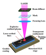 |
| This illustration depicts a new technique that uses a pulsing laser to create synthetic nanodiamond films and patterns from graphite, with potential applications from biosensors to computer chips. Purdue University image/Gary Cheng |
Abstract:
Direct Laser Writing of Nanodiamond Films from Graphite under Ambient Conditions
Qiong Nian, Yuefeng Wang, Yingling Yang, Ji Li, Martin Y. Zhang, Jiayi Shao, Liang Tang & Gary J. Cheng
Purdue University
Synthesis of diamond, a multi-functional material, has been a challenge due to very high activation energy for transforming graphite to diamond, and therefore, has been hindering it from being potentially exploited for novel applications. In this study, we explore a new approach, namely confined pulse laser deposition (CPLD), in which nanosecond laser ablation of graphite within a confinement layer simultaneously activates plasma and effectively confine it to create a favorable condition for nanodiamond formation from graphite. It is noteworthy that due to the local high dense confined plasma created by transparent confinement layer, nanodiamond has been formed at laser intensity as low as 3.7 GW/cm2, which corresponds to pressure of 4.4 GPa, much lower than the pressure needed to transform graphite to diamond traditionally. By manipulating the laser conditions, semi-transparent carbon films with good conductivity (several kΩ/Sq) were also obtained by this method. This technique provides a new channel, from confined plasma to solid, to deposit materials that normally need high temperature and high pressure. This technique has several important advantages to allow scalable processing, such as high speed, direct writing without catalyst, selective and flexible processing, low cost without expensive pico/femtosecond laser systems, high temperature/vacuum chambers.
'Direct writing' of diamond patterns from graphite a potential technological leap
West Lafayette, IN | Posted on November 5th, 2014What began as research into a method to strengthen metals has led to the discovery of a new technique that uses a pulsing laser to create synthetic nanodiamond films and patterns from graphite, with potential applications from biosensors to computer chips.
"The biggest advantage is that you can selectively deposit nanodiamond on rigid surfaces without the high temperatures and pressures normally needed to produce synthetic diamond," said Gary Cheng, an associate professor of industrial engineering at Purdue University. "We do this at room temperature and without a high temperature and pressure chamber, so this process could significantly lower the cost of making diamond. In addition, we realize a direct writing technique that could selectively write nanodiamond in designed patterns."
The ability to selectively "write" lines of diamond on surfaces could be practical for various potential applications including biosensors, quantum computing, fuel cells and next-generation computer chips.
The technique works by using a multilayered film that includes a layer of graphite topped with a glass cover sheet. Exposing this layered structure to an ultrafast-pulsing laser instantly converts the graphite to an ionized plasma and creates a downward pressure. Then the graphite plasma quickly solidifies into diamond. The glass sheet confines the plasma to keep it from escaping, allowing it to form a nanodiamond coating.
"These are super-small diamonds and the coating is super-strong, so it could be used for high-temperature sensors," Cheng said.
Research findings are detailed in a paper that appeared online in the Nature journal Scientific Reports. The paper was authored by former Purdue doctoral students Yuefeng Wang, Yingling Yang, Ji Li and Martin Y. Zhang; postdoctoral research associate Jiayi Shao; doctoral students Qiong Nian and Liang Tang; and Cheng.
The researchers made the discovery while studying how to strengthen metals using a thin layer of graphite and a nanosecond-pulsing laser. A doctoral student noticed that the laser was either causing the graphite to disappear or turn semi-transparent.
"The black coating of graphite was gone, but where did it go?" Cheng said.
Subsequent research proved the graphite had turned into diamond. The Purdue researchers have named the process confined pulse laser deposition (CPLD).
The research team confirmed that the structures are diamond using a variety of techniques including transmission electron microscopy, X-ray diffraction and the measurement of electrical resistance.
A U.S. patent application has been filed on the concept through the Purdue Office of Technology Commercialization. More research is needed to commercialize the technique, Cheng said.
####
For more information, please click here
Contacts:
Writer:
Emil Venere
765-494-4709
Source:
Gary J. Cheng
765-494-5436
Copyright © Purdue University
If you have a comment, please Contact us.Issuers of news releases, not 7th Wave, Inc. or Nanotechnology Now, are solely responsible for the accuracy of the content.
Bookmark:


| Related News Press |
News and information
![]() Simulating magnetization in a Heisenberg quantum spin chain April 5th, 2024
Simulating magnetization in a Heisenberg quantum spin chain April 5th, 2024
![]() NRL charters Navy�s quantum inertial navigation path to reduce drift April 5th, 2024
NRL charters Navy�s quantum inertial navigation path to reduce drift April 5th, 2024
![]() Discovery points path to flash-like memory for storing qubits: Rice find could hasten development of nonvolatile quantum memory April 5th, 2024
Discovery points path to flash-like memory for storing qubits: Rice find could hasten development of nonvolatile quantum memory April 5th, 2024
![]() Good as gold - improving infectious disease testing with gold nanoparticles April 5th, 2024
Good as gold - improving infectious disease testing with gold nanoparticles April 5th, 2024
Thin films
![]() Utilizing palladium for addressing contact issues of buried oxide thin film transistors April 5th, 2024
Utilizing palladium for addressing contact issues of buried oxide thin film transistors April 5th, 2024
![]() Understanding the mechanism of non-uniform formation of diamond film on tools: Paving the way to a dry process with less environmental impact March 24th, 2023
Understanding the mechanism of non-uniform formation of diamond film on tools: Paving the way to a dry process with less environmental impact March 24th, 2023
![]() New study introduces the best graphite films: The work by Distinguished Professor Feng Ding at UNIST has been published in the October 2022 issue of Nature Nanotechnology November 4th, 2022
New study introduces the best graphite films: The work by Distinguished Professor Feng Ding at UNIST has been published in the October 2022 issue of Nature Nanotechnology November 4th, 2022
Chip Technology
![]() Discovery points path to flash-like memory for storing qubits: Rice find could hasten development of nonvolatile quantum memory April 5th, 2024
Discovery points path to flash-like memory for storing qubits: Rice find could hasten development of nonvolatile quantum memory April 5th, 2024
![]() Utilizing palladium for addressing contact issues of buried oxide thin film transistors April 5th, 2024
Utilizing palladium for addressing contact issues of buried oxide thin film transistors April 5th, 2024
![]() HKUST researchers develop new integration technique for efficient coupling of III-V and silicon February 16th, 2024
HKUST researchers develop new integration technique for efficient coupling of III-V and silicon February 16th, 2024
Sensors
Discoveries
![]() Chemical reactions can scramble quantum information as well as black holes April 5th, 2024
Chemical reactions can scramble quantum information as well as black holes April 5th, 2024
![]() New micromaterial releases nanoparticles that selectively destroy cancer cells April 5th, 2024
New micromaterial releases nanoparticles that selectively destroy cancer cells April 5th, 2024
![]() Utilizing palladium for addressing contact issues of buried oxide thin film transistors April 5th, 2024
Utilizing palladium for addressing contact issues of buried oxide thin film transistors April 5th, 2024
Materials/Metamaterials/Magnetoresistance
![]() Nanoscale CL thermometry with lanthanide-doped heavy-metal oxide in TEM March 8th, 2024
Nanoscale CL thermometry with lanthanide-doped heavy-metal oxide in TEM March 8th, 2024
![]() Focused ion beam technology: A single tool for a wide range of applications January 12th, 2024
Focused ion beam technology: A single tool for a wide range of applications January 12th, 2024
Announcements
![]() NRL charters Navy�s quantum inertial navigation path to reduce drift April 5th, 2024
NRL charters Navy�s quantum inertial navigation path to reduce drift April 5th, 2024
![]() Discovery points path to flash-like memory for storing qubits: Rice find could hasten development of nonvolatile quantum memory April 5th, 2024
Discovery points path to flash-like memory for storing qubits: Rice find could hasten development of nonvolatile quantum memory April 5th, 2024
Interviews/Book Reviews/Essays/Reports/Podcasts/Journals/White papers/Posters
![]() Simulating magnetization in a Heisenberg quantum spin chain April 5th, 2024
Simulating magnetization in a Heisenberg quantum spin chain April 5th, 2024
![]() Discovery points path to flash-like memory for storing qubits: Rice find could hasten development of nonvolatile quantum memory April 5th, 2024
Discovery points path to flash-like memory for storing qubits: Rice find could hasten development of nonvolatile quantum memory April 5th, 2024
Tools
![]() Ferroelectrically modulate the Fermi level of graphene oxide to enhance SERS response November 3rd, 2023
Ferroelectrically modulate the Fermi level of graphene oxide to enhance SERS response November 3rd, 2023
![]() The USTC realizes In situ electron paramagnetic resonance spectroscopy using single nanodiamond sensors November 3rd, 2023
The USTC realizes In situ electron paramagnetic resonance spectroscopy using single nanodiamond sensors November 3rd, 2023
Patents/IP/Tech Transfer/Licensing
![]() Getting drugs across the blood-brain barrier using nanoparticles March 3rd, 2023
Getting drugs across the blood-brain barrier using nanoparticles March 3rd, 2023
![]() Metasurfaces control polarized light at will: New research unlocks the hidden potential of metasurfaces August 13th, 2021
Metasurfaces control polarized light at will: New research unlocks the hidden potential of metasurfaces August 13th, 2021
![]() Arrowhead Pharmaceuticals Announces Closing of Agreement with Takeda November 27th, 2020
Arrowhead Pharmaceuticals Announces Closing of Agreement with Takeda November 27th, 2020
Photonics/Optics/Lasers
![]() With VECSELs towards the quantum internet Fraunhofer: IAF achieves record output power with VECSEL for quantum frequency converters April 5th, 2024
With VECSELs towards the quantum internet Fraunhofer: IAF achieves record output power with VECSEL for quantum frequency converters April 5th, 2024
![]() Nanoscale CL thermometry with lanthanide-doped heavy-metal oxide in TEM March 8th, 2024
Nanoscale CL thermometry with lanthanide-doped heavy-metal oxide in TEM March 8th, 2024
![]() Optically trapped quantum droplets of light can bind together to form macroscopic complexes March 8th, 2024
Optically trapped quantum droplets of light can bind together to form macroscopic complexes March 8th, 2024
![]() HKUST researchers develop new integration technique for efficient coupling of III-V and silicon February 16th, 2024
HKUST researchers develop new integration technique for efficient coupling of III-V and silicon February 16th, 2024
|
|
||
|
|
||
| The latest news from around the world, FREE | ||
|
|
||
|
|
||
| Premium Products | ||
|
|
||
|
Only the news you want to read!
Learn More |
||
|
|
||
|
Full-service, expert consulting
Learn More |
||
|
|
||