Home > Press > A Crystal Wedding in the Nanocosmos
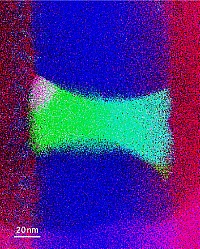 |
| Indium arsenide (green-cyan) is perfectly integrated into the silicon nanowire (blue). (Energy-dispersive X-ray spectroscopy). Photo: HZDR/Prucnal |
Abstract:
Researchers at the Helmholtz-Zentrum Dresden-Rossendorf (HZDR), the Vienna University of Technology and the Maria Curie-Skłodowska University Lublin have succeeded in embedding nearly perfect semiconductor crystals into a silicon nanowire. With this new method of producing hybrid nanowires, very fast and multi-functional processing units can be accommodated on a single chip in the future. The research results will be published in the journal Nano Research.
A Crystal Wedding in the Nanocosmos
Dresden, Germany | Posted on July 23rd, 2014Nano-optoelectronics are considered the cornerstone of future chip technology, but the research faces major challenges: on the one hand, electronic components must be accommodated into smaller and smaller spaces. On the other hand, what are known as compound semiconductors are to be embedded into conventional materials. In contrast to silicon, many of such semiconductors with extremely high electron mobility could improve performance of the most modern silicon-based CMOS technology.
Scientists from the HZDR, Vienna University of Technology and Maria Curie-Skłodowska University Lublin have now come a step closer to both these targets: they integrated compound semiconductor crystals made of indium arsenide (InAs) into silicon nanowires, which are ideally suited for constructing increasingly compact chips.
This integration of crystals was the greatest obstacle for such "hetero-nanowires" until now: beyond the nanometer range, crystal lattice mismatch always led to numerous defects. The researchers have now managed a near-perfect production and embedding of the InAs crystals into the nanowires for the first time.
Implanted atoms form crystals in the liquid-phase
In order to carry out this process, ion beam synthesis and heat treatment with xenon flash-lamps were used, two technologies in which the Ion Beam Center of the HZDR has held experience for many years. The scientists initially needed to introduce a determined number of atoms precisely into the wires using ion implantation. They then carried out the flash-lamp annealing of the silicon wires in their liquid-phase within a matter of only twenty milliseconds. "A silicon oxide shell, measuring merely fifteen-nanometers-thick, maintains the form of the liquid nanowire," explains HZDR scientist Dr. Slawomir Prucnal, "while the implanted atoms form the indium-arsenide crystals."
Dr. Wolfgang Skorupa, the head of the research group adds: "The atoms diffuse in the liquid-silicon-phase so rapidly that within milliseconds they form flawless mono-crystals delineated from their surroundings with nearly perfect interfaces." In the next step, the scientists want to implement different compound semiconductors into Silicon nanowires and also optimize the size and distribution of the crystals.
Publication: Prucnal, S. et al. (just accepted, 7/2014). III-V semiconductor nanocrystal formation in silicon nanowires via liquid-phase epitaxy. Nano Research. DOI 10.1007/s12274-014-0536-6
####
For more information, please click here
Contacts:
Christine Bohnet
49-351-260-2450
Dr. Slawomir Prucnal
The Institute of Ion Beam Physics and Materials Research at the HZDR
Tel. +49 351 260 2065
Copyright © Helmholtz-Zentrum Dresden-Rossendorf
If you have a comment, please Contact us.Issuers of news releases, not 7th Wave, Inc. or Nanotechnology Now, are solely responsible for the accuracy of the content.
Bookmark:


| Related News Press |
News and information
![]() Simulating magnetization in a Heisenberg quantum spin chain April 5th, 2024
Simulating magnetization in a Heisenberg quantum spin chain April 5th, 2024
![]() NRL charters Navy�s quantum inertial navigation path to reduce drift April 5th, 2024
NRL charters Navy�s quantum inertial navigation path to reduce drift April 5th, 2024
![]() Discovery points path to flash-like memory for storing qubits: Rice find could hasten development of nonvolatile quantum memory April 5th, 2024
Discovery points path to flash-like memory for storing qubits: Rice find could hasten development of nonvolatile quantum memory April 5th, 2024
Chip Technology
![]() Discovery points path to flash-like memory for storing qubits: Rice find could hasten development of nonvolatile quantum memory April 5th, 2024
Discovery points path to flash-like memory for storing qubits: Rice find could hasten development of nonvolatile quantum memory April 5th, 2024
![]() Utilizing palladium for addressing contact issues of buried oxide thin film transistors April 5th, 2024
Utilizing palladium for addressing contact issues of buried oxide thin film transistors April 5th, 2024
![]() HKUST researchers develop new integration technique for efficient coupling of III-V and silicon February 16th, 2024
HKUST researchers develop new integration technique for efficient coupling of III-V and silicon February 16th, 2024
Nanoelectronics
![]() Interdisciplinary: Rice team tackles the future of semiconductors Multiferroics could be the key to ultralow-energy computing October 6th, 2023
Interdisciplinary: Rice team tackles the future of semiconductors Multiferroics could be the key to ultralow-energy computing October 6th, 2023
![]() Key element for a scalable quantum computer: Physicists from Forschungszentrum J�lich and RWTH Aachen University demonstrate electron transport on a quantum chip September 23rd, 2022
Key element for a scalable quantum computer: Physicists from Forschungszentrum J�lich and RWTH Aachen University demonstrate electron transport on a quantum chip September 23rd, 2022
![]() Reduced power consumption in semiconductor devices September 23rd, 2022
Reduced power consumption in semiconductor devices September 23rd, 2022
![]() Atomic level deposition to extend Moore�s law and beyond July 15th, 2022
Atomic level deposition to extend Moore�s law and beyond July 15th, 2022
Discoveries
![]() Chemical reactions can scramble quantum information as well as black holes April 5th, 2024
Chemical reactions can scramble quantum information as well as black holes April 5th, 2024
![]() New micromaterial releases nanoparticles that selectively destroy cancer cells April 5th, 2024
New micromaterial releases nanoparticles that selectively destroy cancer cells April 5th, 2024
![]() Utilizing palladium for addressing contact issues of buried oxide thin film transistors April 5th, 2024
Utilizing palladium for addressing contact issues of buried oxide thin film transistors April 5th, 2024
Announcements
![]() NRL charters Navy�s quantum inertial navigation path to reduce drift April 5th, 2024
NRL charters Navy�s quantum inertial navigation path to reduce drift April 5th, 2024
![]() Discovery points path to flash-like memory for storing qubits: Rice find could hasten development of nonvolatile quantum memory April 5th, 2024
Discovery points path to flash-like memory for storing qubits: Rice find could hasten development of nonvolatile quantum memory April 5th, 2024
Interviews/Book Reviews/Essays/Reports/Podcasts/Journals/White papers/Posters
![]() Simulating magnetization in a Heisenberg quantum spin chain April 5th, 2024
Simulating magnetization in a Heisenberg quantum spin chain April 5th, 2024
![]() Discovery points path to flash-like memory for storing qubits: Rice find could hasten development of nonvolatile quantum memory April 5th, 2024
Discovery points path to flash-like memory for storing qubits: Rice find could hasten development of nonvolatile quantum memory April 5th, 2024
Research partnerships
![]() Discovery points path to flash-like memory for storing qubits: Rice find could hasten development of nonvolatile quantum memory April 5th, 2024
Discovery points path to flash-like memory for storing qubits: Rice find could hasten development of nonvolatile quantum memory April 5th, 2024
![]() Researchers� approach may protect quantum computers from attacks March 8th, 2024
Researchers� approach may protect quantum computers from attacks March 8th, 2024
![]() 'Sudden death' of quantum fluctuations defies current theories of superconductivity: Study challenges the conventional wisdom of superconducting quantum transitions January 12th, 2024
'Sudden death' of quantum fluctuations defies current theories of superconductivity: Study challenges the conventional wisdom of superconducting quantum transitions January 12th, 2024
|
|
||
|
|
||
| The latest news from around the world, FREE | ||
|
|
||
|
|
||
| Premium Products | ||
|
|
||
|
Only the news you want to read!
Learn More |
||
|
|
||
|
Full-service, expert consulting
Learn More |
||
|
|
||