Home > Press > Caltech Researchers Create Light-Bending Silicon Chip: Bending the Light with a Tiny Chip
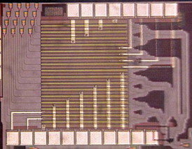 |
| An image of Hajimiri's light-bending silicon chip. Credit: Ali Hajimiri/Caltech |
Abstract:
Imagine that you are in a meeting with coworkers or at a gathering of friends. You pull out your cell phone to show a presentation or a video on YouTube. But you don't use the tiny screen; your phone projects a bright, clear image onto a wall or a big screen. Such a technology may be on its way, thanks to a new light-bending silicon chip developed by researchers at Caltech.
The letters "C," "I," and "T" projected using Hajimiri's optical phased array chip. The images shown were projected in infrared light.
Credit: Ali Hajimiri/Caltech
Caltech Researchers Create Light-Bending Silicon Chip: Bending the Light with a Tiny Chip
Pasadena, CA | Posted on March 10th, 2014The chip was developed by Ali Hajimiri, Thomas G. Myers Professor of Electrical Engineering, and researchers in his laboratory. The results were presented at the Optical Fiber Communication (OFC) conference in San Francisco on March 10.
Traditional projectors�like those used to project a film or classroom lecture notes�pass a beam of light through a tiny image, using lenses to map each point of the small picture to corresponding, yet expanded, points on a large screen. The Caltech chip eliminates the need for bulky and expensive lenses and bulbs and instead uses a so-called integrated optical phased array (OPA) to project the image electronically with only a single laser diode as light source and no mechanically moving parts.
Hajimiri and his colleagues were able to bypass traditional optics by manipulating the coherence of light�a property that allows the researchers to "bend" the light waves on the surface of the chip without lenses or the use of any mechanical movement. If two waves are coherent in the direction of propagation�meaning that the peaks and troughs of one wave are exactly aligned with those of the second wave�the waves combine, resulting in one wave, a beam with twice the amplitude and four times the energy as the initial wave, moving in the direction of the coherent waves.
"By changing the relative timing of the waves, you can change the direction of the light beam," says Hajimiri. For example, if 10 people kneeling in line by a swimming pool slap the water at the exact same instant, they will make one big wave that travels directly away from them. But if the 10 separate slaps are staggered�each person hitting the water a half a second after the last�there will still be one big, combined wave, but with the wave bending to travel at an angle, he says.
Using a series of pipes for the light�called phase shifters�the OPA chip similarly slows down or speeds up the timing of the waves, thus controlling the direction of the light beam. To form an image, electronic data from a computer are converted into multiple electrical currents; by applying stronger or weaker currents to the light within the phase shifter, the number of electrons within each light path changes�which, in turn, changes the timing of the light wave in that path. The timed light waves are then delivered to tiny array elements within a grid on the chip. The light is then projected from each array in the grid, the individual array beams combining coherently in the air to form a single light beam and a spot on the screen.
As the electronic signal rapidly steers the beam left, right, up, and down, the light acts as a very fast pen, drawing an image made of light on the projection surface. Because the direction of the light beam is controlled electronically�not mechanically�it can create a sort of line very quickly. Since the light draws many times per second, the eye sees the process as a single image instead of a moving light beam, says Hajimiri.
"The new thing about our work is really that we can do this on a tiny, one-millimeter-square silicon chip, and the fact that we can do it very rapidly�rapidly enough to form images, since we phase-shift electronically in two dimensions," says Behrooz Abiri, a graduate student in Hajimiri's group and a coauthor on the paper. So far, the images Hajimiri and his team can project with the current version of the chip are somewhat simple�a triangle, a smiley face, or single letters, for example. However, the researchers are currently experimenting with larger chips that include more light-delivering array elements that�like using a larger lens on a camera�can improve the resolution and increase the complexity of the projected images.
In their recent experiments, Hajimiri and his colleagues have used the silicon chip to project images in infrared light, but additional work with different types of semiconductors will also allow the researchers to expand the tiny projector's capabilities into the visible spectrum. "Right now we are using silicon technology, which works better with infrared light. If you want to project visible light, you can take the exact same architecture and do it in what's called compound semiconductor III-V technology," says Firooz Aflatouni, another coauthor on the paper, who in January finished his two-year postdoctoral appointment at Caltech and joined the University of Pennsylvania as an assistant professor. "Silicon is good because it can be easily integrated into electronics, but these other compound semiconductors could be used to do the same thing."
"In the future, this can be incorporated into a phone, and since there is no need for a lens, you can have a phone that acts as a projector all by itself," Hajimiri says. However, although the chip could easily be incorporated into a cell phone, he points out that a tiny projection device can have many applications�including light-based radar systems (called "LIDAR"), which are used in positioning, robotics, geographical measurements, and mapmaking. Such equipment already exists, but current LIDAR technology requires complex, bulky, and expensive equipment�equipment that could be streamlined and simplified to a single chip at a much lower cost.
"But I don't want to limit the device to just a few purposes. The beauty of this thing is that these chips are small and can be made at a very low cost�and this opens up lots of interesting possibilities," he says.
These results were described in a presentation titled "Electronic Two-Dimensional Beam Steering for Integrated Optical Phased Arrays." Along with Hajimiri, Abiri, and Aflatouni, Caltech senior Angad Rekhi is also a coauthor on this paper. The work was funded by grants from the Caltech Innovation Initiative, and the Information Science and Technology initiative at Caltech.
# # #
Written by Jessica Stoller-Conrad
####
For more information, please click here
Contacts:
Brian Bell
(626) 395-5832
Copyright © Caltech
If you have a comment, please Contact us.Issuers of news releases, not 7th Wave, Inc. or Nanotechnology Now, are solely responsible for the accuracy of the content.
Bookmark:


| Related News Press |
News and information
![]() Simulating magnetization in a Heisenberg quantum spin chain April 5th, 2024
Simulating magnetization in a Heisenberg quantum spin chain April 5th, 2024
![]() NRL charters Navy�s quantum inertial navigation path to reduce drift April 5th, 2024
NRL charters Navy�s quantum inertial navigation path to reduce drift April 5th, 2024
![]() Discovery points path to flash-like memory for storing qubits: Rice find could hasten development of nonvolatile quantum memory April 5th, 2024
Discovery points path to flash-like memory for storing qubits: Rice find could hasten development of nonvolatile quantum memory April 5th, 2024
Videos/Movies
![]() New X-ray imaging technique to study the transient phases of quantum materials December 29th, 2022
New X-ray imaging technique to study the transient phases of quantum materials December 29th, 2022
![]() Solvent study solves solar cell durability puzzle: Rice-led project could make perovskite cells ready for prime time September 23rd, 2022
Solvent study solves solar cell durability puzzle: Rice-led project could make perovskite cells ready for prime time September 23rd, 2022
![]() Scientists prepare for the world�s smallest race: Nanocar Race II March 18th, 2022
Scientists prepare for the world�s smallest race: Nanocar Race II March 18th, 2022
![]() Visualizing the invisible: New fluorescent DNA label reveals nanoscopic cancer features March 4th, 2022
Visualizing the invisible: New fluorescent DNA label reveals nanoscopic cancer features March 4th, 2022
Ethics
![]() Artificial Intelligence Centered Cancer Nanomedicine: Diagnostics, Therapeutics and Bioethics June 3rd, 2022
Artificial Intelligence Centered Cancer Nanomedicine: Diagnostics, Therapeutics and Bioethics June 3rd, 2022
![]() Iran to hold intl. school on application of nanomaterials in medicine September 20th, 2016
Iran to hold intl. school on application of nanomaterials in medicine September 20th, 2016
![]() Synthetic biology needs robust safety mechanisms before real world application: Ethics and technology hold the key to the success of synthetic biology September 17th, 2015
Synthetic biology needs robust safety mechanisms before real world application: Ethics and technology hold the key to the success of synthetic biology September 17th, 2015
![]() March 2016; 6th Int'l Conference on Nanostructures in Iran July 29th, 2015
March 2016; 6th Int'l Conference on Nanostructures in Iran July 29th, 2015
Discoveries
![]() Chemical reactions can scramble quantum information as well as black holes April 5th, 2024
Chemical reactions can scramble quantum information as well as black holes April 5th, 2024
![]() New micromaterial releases nanoparticles that selectively destroy cancer cells April 5th, 2024
New micromaterial releases nanoparticles that selectively destroy cancer cells April 5th, 2024
![]() Utilizing palladium for addressing contact issues of buried oxide thin film transistors April 5th, 2024
Utilizing palladium for addressing contact issues of buried oxide thin film transistors April 5th, 2024
Announcements
![]() NRL charters Navy�s quantum inertial navigation path to reduce drift April 5th, 2024
NRL charters Navy�s quantum inertial navigation path to reduce drift April 5th, 2024
![]() Discovery points path to flash-like memory for storing qubits: Rice find could hasten development of nonvolatile quantum memory April 5th, 2024
Discovery points path to flash-like memory for storing qubits: Rice find could hasten development of nonvolatile quantum memory April 5th, 2024
Interviews/Book Reviews/Essays/Reports/Podcasts/Journals/White papers/Posters
![]() Simulating magnetization in a Heisenberg quantum spin chain April 5th, 2024
Simulating magnetization in a Heisenberg quantum spin chain April 5th, 2024
![]() Discovery points path to flash-like memory for storing qubits: Rice find could hasten development of nonvolatile quantum memory April 5th, 2024
Discovery points path to flash-like memory for storing qubits: Rice find could hasten development of nonvolatile quantum memory April 5th, 2024
Events/Classes
![]() Researchers demonstrate co-propagation of quantum and classical signals: Study shows that quantum encryption can be implemented in existing fiber networks January 20th, 2023
Researchers demonstrate co-propagation of quantum and classical signals: Study shows that quantum encryption can be implemented in existing fiber networks January 20th, 2023
Grants/Sponsored Research/Awards/Scholarships/Gifts/Contests/Honors/Records
![]() Discovery points path to flash-like memory for storing qubits: Rice find could hasten development of nonvolatile quantum memory April 5th, 2024
Discovery points path to flash-like memory for storing qubits: Rice find could hasten development of nonvolatile quantum memory April 5th, 2024
![]() Chemical reactions can scramble quantum information as well as black holes April 5th, 2024
Chemical reactions can scramble quantum information as well as black holes April 5th, 2024
Photonics/Optics/Lasers
![]() With VECSELs towards the quantum internet Fraunhofer: IAF achieves record output power with VECSEL for quantum frequency converters April 5th, 2024
With VECSELs towards the quantum internet Fraunhofer: IAF achieves record output power with VECSEL for quantum frequency converters April 5th, 2024
![]() Nanoscale CL thermometry with lanthanide-doped heavy-metal oxide in TEM March 8th, 2024
Nanoscale CL thermometry with lanthanide-doped heavy-metal oxide in TEM March 8th, 2024
![]() Optically trapped quantum droplets of light can bind together to form macroscopic complexes March 8th, 2024
Optically trapped quantum droplets of light can bind together to form macroscopic complexes March 8th, 2024
![]() HKUST researchers develop new integration technique for efficient coupling of III-V and silicon February 16th, 2024
HKUST researchers develop new integration technique for efficient coupling of III-V and silicon February 16th, 2024
|
|
||
|
|
||
| The latest news from around the world, FREE | ||
|
|
||
|
|
||
| Premium Products | ||
|
|
||
|
Only the news you want to read!
Learn More |
||
|
|
||
|
Full-service, expert consulting
Learn More |
||
|
|
||