Home > Press > New 2D material for next generation high-speed electronics
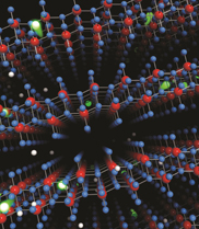 |
| Artist impression of high carrier mobility through layered molybdenum oxide crystal lattice. Credit: Dr Daniel J White, ScienceFX |
Abstract:
Scientists at CSIRO and RMIT University have produced a new two-dimensional material that could revolutionise the electronics market, making "nano" more than just a marketing term.
New 2D material for next generation high-speed electronics
Clayton, Australia | Posted on January 22nd, 2013The material - made up of layers of crystal known as molybdenum oxides - has unique properties that encourage the free flow of electrons at ultra-high speeds.
In a paper published in the January issue of materials science journal Advanced Materials, the researchers explain how they adapted a revolutionary material known as graphene to create a new conductive nano-material.
Graphene was created in 2004 by scientists in the UK and won its inventors a Nobel Prize in 2010. While graphene supports high speed electrons, its physical properties prevent it from being used for high-speed electronics.
The CSIRO's Dr Serge Zhuiykov said the new nano-material was made up of layered sheets - similar to graphite layers that make up a pencil's core.
"Within these layers, electrons are able to zip through at high speeds with minimal scattering," Dr Zhuiykov said.
"The importance of our breakthrough is how quickly and fluently electrons - which conduct electricity - are able to flow through the new material."
RMIT's Professor Kourosh Kalantar-zadeh said the researchers were able to remove "road blocks" that could obstruct the electrons, an essential step for the development of high-speed electronics.
"Instead of scattering when they hit road blocks, as they would in conventional materials, they can simply pass through this new material and get through the structure faster," Professor Kalantar-zadeh said.
"Quite simply, if electrons can pass through a structure quicker, we can build devices that are smaller and transfer data at much higher speeds.
"While more work needs to be done before we can develop actual gadgets using this new 2D nano-material, this breakthrough lays the foundation for a new electronics revolution and we look forward to exploring its potential."
In the paper titled 'Enhanced Charge Carrier Mobility in Two-Dimensional High Dielectric Molybdenum Oxide,' the researchers describe how they used a process known as "exfoliation" to create layers of the material ~11 nm thick.
The material was manipulated to convert it into a semiconductor and nanoscale transistors were then created using molybdenum oxide.
The result was electron mobility values of >1,100 cm2/Vs - exceeding the current industry standard for low dimensional silicon.
The work, with RMIT doctoral researcher Sivacarendran Balendhran as the lead author, was supported by the CSIRO Sensors and Sensor Networks Transformational Capability Platform and the CSIRO Materials Science and Engineering Division.
It was also a result of collaboration between researchers from Monash University, University of California - Los Angeles (UCLA), CSIRO, Massachusetts Institute of Technology (MIT) and RMIT.
####
For more information, please click here
Contacts:
Simon Hunter
61-395-458-412
Copyright © CSIRO Australia
If you have a comment, please Contact us.Issuers of news releases, not 7th Wave, Inc. or Nanotechnology Now, are solely responsible for the accuracy of the content.
Bookmark:


| Related News Press |
News and information
![]() Simulating magnetization in a Heisenberg quantum spin chain April 5th, 2024
Simulating magnetization in a Heisenberg quantum spin chain April 5th, 2024
![]() NRL charters Navy�s quantum inertial navigation path to reduce drift April 5th, 2024
NRL charters Navy�s quantum inertial navigation path to reduce drift April 5th, 2024
![]() Discovery points path to flash-like memory for storing qubits: Rice find could hasten development of nonvolatile quantum memory April 5th, 2024
Discovery points path to flash-like memory for storing qubits: Rice find could hasten development of nonvolatile quantum memory April 5th, 2024
Chip Technology
![]() Discovery points path to flash-like memory for storing qubits: Rice find could hasten development of nonvolatile quantum memory April 5th, 2024
Discovery points path to flash-like memory for storing qubits: Rice find could hasten development of nonvolatile quantum memory April 5th, 2024
![]() Utilizing palladium for addressing contact issues of buried oxide thin film transistors April 5th, 2024
Utilizing palladium for addressing contact issues of buried oxide thin film transistors April 5th, 2024
![]() HKUST researchers develop new integration technique for efficient coupling of III-V and silicon February 16th, 2024
HKUST researchers develop new integration technique for efficient coupling of III-V and silicon February 16th, 2024
Nanoelectronics
![]() Interdisciplinary: Rice team tackles the future of semiconductors Multiferroics could be the key to ultralow-energy computing October 6th, 2023
Interdisciplinary: Rice team tackles the future of semiconductors Multiferroics could be the key to ultralow-energy computing October 6th, 2023
![]() Key element for a scalable quantum computer: Physicists from Forschungszentrum J�lich and RWTH Aachen University demonstrate electron transport on a quantum chip September 23rd, 2022
Key element for a scalable quantum computer: Physicists from Forschungszentrum J�lich and RWTH Aachen University demonstrate electron transport on a quantum chip September 23rd, 2022
![]() Reduced power consumption in semiconductor devices September 23rd, 2022
Reduced power consumption in semiconductor devices September 23rd, 2022
![]() Atomic level deposition to extend Moore�s law and beyond July 15th, 2022
Atomic level deposition to extend Moore�s law and beyond July 15th, 2022
Discoveries
![]() Chemical reactions can scramble quantum information as well as black holes April 5th, 2024
Chemical reactions can scramble quantum information as well as black holes April 5th, 2024
![]() New micromaterial releases nanoparticles that selectively destroy cancer cells April 5th, 2024
New micromaterial releases nanoparticles that selectively destroy cancer cells April 5th, 2024
![]() Utilizing palladium for addressing contact issues of buried oxide thin film transistors April 5th, 2024
Utilizing palladium for addressing contact issues of buried oxide thin film transistors April 5th, 2024
Announcements
![]() NRL charters Navy�s quantum inertial navigation path to reduce drift April 5th, 2024
NRL charters Navy�s quantum inertial navigation path to reduce drift April 5th, 2024
![]() Discovery points path to flash-like memory for storing qubits: Rice find could hasten development of nonvolatile quantum memory April 5th, 2024
Discovery points path to flash-like memory for storing qubits: Rice find could hasten development of nonvolatile quantum memory April 5th, 2024
Research partnerships
![]() Discovery points path to flash-like memory for storing qubits: Rice find could hasten development of nonvolatile quantum memory April 5th, 2024
Discovery points path to flash-like memory for storing qubits: Rice find could hasten development of nonvolatile quantum memory April 5th, 2024
![]() Researchers� approach may protect quantum computers from attacks March 8th, 2024
Researchers� approach may protect quantum computers from attacks March 8th, 2024
![]() 'Sudden death' of quantum fluctuations defies current theories of superconductivity: Study challenges the conventional wisdom of superconducting quantum transitions January 12th, 2024
'Sudden death' of quantum fluctuations defies current theories of superconductivity: Study challenges the conventional wisdom of superconducting quantum transitions January 12th, 2024
|
|
||
|
|
||
| The latest news from around the world, FREE | ||
|
|
||
|
|
||
| Premium Products | ||
|
|
||
|
Only the news you want to read!
Learn More |
||
|
|
||
|
Full-service, expert consulting
Learn More |
||
|
|
||