Home > Press > NRL Demonstrates High Durability of Nanotube Transistors to the Harsh Space Environment
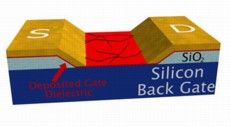 |
| A locally etched back-gated field effect transistor (FET) structure with a deposited dielectric layer. Thick dielectric layers are highly susceptible to radiation induced charge build-up, which is known to cause threshold voltage shifts and increased leakage in metal-oxide semiconductor (MOS) devices. To mitigate these effects, the dielectric layer is locally etched in the active region of the back-gated FET. A gate dielectric material is then deposited (depicted in red) over the entire substrate. (Photo: U.S. Naval Research Laboratory) |
Abstract:
U.S. Naval Research Laboratory electronics science and technology engineers demonstrate the ability of single walled carbon nanotube transistors (SWCNTs) to survive the harsh space environment, investigating the effects of ionizing radiation on the crystalline structures and further supporting the development of SWCNT-based nanoelectronics for use in harsh radiation environments.
NRL Demonstrates High Durability of Nanotube Transistors to the Harsh Space Environment
Washington, DC | Posted on September 21st, 2012"One of the primary challenges for space electronics is mitigating the susceptibility of prolonged exposure to radiation that exists in the charged particle belts that encircle Earth," said Cory Cress, materials research engineer. "These are the first controlled demonstrations showing little performance degradation and high tolerance to cumulative ionizing radiation exposure."
Radiation effects take two forms, transient effects and cumulative effects. The former, referred to as single effect transients (SETs), result from a direct strike by an ionizing particle in space that causes a current pulse in the device. If this pulse propagates through the circuit it can cause data corruption that can be extremely detrimental to someone that relies on that signal, such as a person using GPS for navigation. NRL researchers have recently predicted that such effects are nearly eliminated for SWCNT-based nanoelectronics due to their small size, low density, and inherent isolation from neighboring SWCNTs in a device.
The cumulative effects in traditional electronics results from trapped charges in the oxides of the devices, including the gate oxide and those used to isolate adjacent devices, the latter being primary source of radiation-induced performance degradation in state-of-the-art complementary metal-oxide semiconductor (CMOS) devices. The effect is manifested as a shift in the voltage needed to turn the transistor on or off. This initially results in power leakage, but can eventually cause failure of the entire circuit.
By developing a SWCNT structure with a thin gate oxide made from thin silicon oxynitride, NRL researchers recently demonstrated SWCNT transistors that do not suffer from such radiation-induced performance changes. This hardened dielectric material and naturally isolated one-dimensional SWCNT structure makes them extremely radiation tolerant.
The ability for SWCNT-based transistors to be both tolerant to transient and cumulative effects potentially enables future space electronics with less redundancy and error-correction circuitry, while maintaining the same quality of fidelity. This reduction in overhead alone would greatly reduce power and improve performance over existing space-electronic systems even if the SWCNT-based transistors operate at the same speed as current technologies. Even greater benefits are foreseeable in the future, once devices are developed that exceed the performance of silicon-based transistors.
####
About U.S. Naval Research Laboratory
The U.S. Naval Research Laboratory is the Navy's full-spectrum corporate laboratory, conducting a broadly based multidisciplinary program of scientific research and advanced technological development. The Laboratory, with a total complement of nearly 2,500 personnel, is located in southwest Washington, D.C., with other major sites at the Stennis Space Center, Miss., and Monterey, Calif. NRL has served the Navy and the nation for over 85 years and continues to meet the complex technological challenges of today's world. For more information, visit the NRL homepage or join the conversation on Twitter, Facebook, and YouTube.
For more information, please click here
Contacts:
U.S. Naval Research Laboratory
Daniel Parry, 202-767-2541
Copyright © U.S. Naval Research Laboratory
If you have a comment, please Contact us.Issuers of news releases, not 7th Wave, Inc. or Nanotechnology Now, are solely responsible for the accuracy of the content.
Bookmark:


| Related News Press |
News and information
![]() Simulating magnetization in a Heisenberg quantum spin chain April 5th, 2024
Simulating magnetization in a Heisenberg quantum spin chain April 5th, 2024
![]() NRL charters Navy�s quantum inertial navigation path to reduce drift April 5th, 2024
NRL charters Navy�s quantum inertial navigation path to reduce drift April 5th, 2024
![]() Discovery points path to flash-like memory for storing qubits: Rice find could hasten development of nonvolatile quantum memory April 5th, 2024
Discovery points path to flash-like memory for storing qubits: Rice find could hasten development of nonvolatile quantum memory April 5th, 2024
Laboratories
![]() A battery�s hopping ions remember where they�ve been: Seen in atomic detail, the seemingly smooth flow of ions through a battery�s electrolyte is surprisingly complicated February 16th, 2024
A battery�s hopping ions remember where they�ve been: Seen in atomic detail, the seemingly smooth flow of ions through a battery�s electrolyte is surprisingly complicated February 16th, 2024
![]() NRL discovers two-dimensional waveguides February 16th, 2024
NRL discovers two-dimensional waveguides February 16th, 2024
![]() Three-pronged approach discerns qualities of quantum spin liquids November 17th, 2023
Three-pronged approach discerns qualities of quantum spin liquids November 17th, 2023
Govt.-Legislation/Regulation/Funding/Policy
![]() NRL charters Navy�s quantum inertial navigation path to reduce drift April 5th, 2024
NRL charters Navy�s quantum inertial navigation path to reduce drift April 5th, 2024
![]() Discovery points path to flash-like memory for storing qubits: Rice find could hasten development of nonvolatile quantum memory April 5th, 2024
Discovery points path to flash-like memory for storing qubits: Rice find could hasten development of nonvolatile quantum memory April 5th, 2024
![]() Chemical reactions can scramble quantum information as well as black holes April 5th, 2024
Chemical reactions can scramble quantum information as well as black holes April 5th, 2024
Chip Technology
![]() Discovery points path to flash-like memory for storing qubits: Rice find could hasten development of nonvolatile quantum memory April 5th, 2024
Discovery points path to flash-like memory for storing qubits: Rice find could hasten development of nonvolatile quantum memory April 5th, 2024
![]() Utilizing palladium for addressing contact issues of buried oxide thin film transistors April 5th, 2024
Utilizing palladium for addressing contact issues of buried oxide thin film transistors April 5th, 2024
![]() HKUST researchers develop new integration technique for efficient coupling of III-V and silicon February 16th, 2024
HKUST researchers develop new integration technique for efficient coupling of III-V and silicon February 16th, 2024
Nanotubes/Buckyballs/Fullerenes/Nanorods/Nanostrings
![]() Tests find no free-standing nanotubes released from tire tread wear September 8th, 2023
Tests find no free-standing nanotubes released from tire tread wear September 8th, 2023
![]() Detection of bacteria and viruses with fluorescent nanotubes July 21st, 2023
Detection of bacteria and viruses with fluorescent nanotubes July 21st, 2023
Announcements
![]() NRL charters Navy�s quantum inertial navigation path to reduce drift April 5th, 2024
NRL charters Navy�s quantum inertial navigation path to reduce drift April 5th, 2024
![]() Discovery points path to flash-like memory for storing qubits: Rice find could hasten development of nonvolatile quantum memory April 5th, 2024
Discovery points path to flash-like memory for storing qubits: Rice find could hasten development of nonvolatile quantum memory April 5th, 2024
Military
![]() NRL charters Navy�s quantum inertial navigation path to reduce drift April 5th, 2024
NRL charters Navy�s quantum inertial navigation path to reduce drift April 5th, 2024
![]() What heat can tell us about battery chemistry: using the Peltier effect to study lithium-ion cells March 8th, 2024
What heat can tell us about battery chemistry: using the Peltier effect to study lithium-ion cells March 8th, 2024
![]() New chip opens door to AI computing at light speed February 16th, 2024
New chip opens door to AI computing at light speed February 16th, 2024
Aerospace/Space
![]() Under pressure - space exploration in our time: Advancing space exploration through diverse collaborations and ethical policies February 16th, 2024
Under pressure - space exploration in our time: Advancing space exploration through diverse collaborations and ethical policies February 16th, 2024
![]() Bridging light and electrons January 12th, 2024
Bridging light and electrons January 12th, 2024
![]() Manufacturing advances bring material back in vogue January 20th, 2023
Manufacturing advances bring material back in vogue January 20th, 2023
|
|
||
|
|
||
| The latest news from around the world, FREE | ||
|
|
||
|
|
||
| Premium Products | ||
|
|
||
|
Only the news you want to read!
Learn More |
||
|
|
||
|
Full-service, expert consulting
Learn More |
||
|
|
||