Home > Press > NANOSENSORS™ introduces new Wear Resistant Conductive AFM Probe Series
 |
Abstract:
NANOSENSORS™ introduces a brand new innovative probes series of wear resistant and highly conductive AFM tips with an additionally slightly increased sharpness compared to metal coated AFM probes.
NANOSENSORS™ introduces new Wear Resistant Conductive AFM Probe Series
Neuchâtel, Switzerland | Posted on March 31st, 2012NANOSENSORS™ announced that the first two types of a new innovative SPM probes series of wear resistant and highly conductive AFM tips will be introduced today.
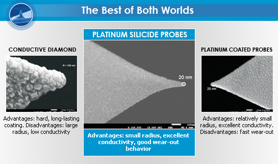
The new AFM probes feature the best of both worlds of the most commonly used conductive probes for Atomic Force Microscopy (AFM): metal coated probes and probes with conductive diamond coating.
The newly developed AFM tips are made of highly conductive platinum silicide which unites high conductivity (higher than conductive diamond coating and as good as metal coated tips) with a high wear resistance (much higher than metal coated probes and almost as good as diamond coated probes).
Additionally the new PtSi probes have a slightly decreased tip radius compared to standard metal coated AFM probes. They can be used for any kind of electric or electrostatic AFM measurement, except SSRM.
The Platinum Silicide AFM probes can be used for:
• TUNA, Tunneling AFM
• SCM, Scanning Capacitance AFM
• C-AFM, Conductive AFM
• EFM, Electrostatic Force Measurements
• KPFM, Kelvin Probe Force Measurements
The first types PtSi-NCH (for non-contact mode) and PtSi-FM (for force modulation mode) are now commercially available.
Further types such as AFM probes for conductive contact mode made of the new material and probes for specialized applications like SSRM are under development.
####
About NANOSENSORS
NANOSENSORS™ is specializing in the development and production of innovative high quality probes for scanning probe microscopy (SPM) and atomic force microscopy (AFM). The products are especially designed for scientists at universities, research institutions and industrial R&D centres in the fields of nanotechnology, microtechnology, materials research, semiconductors, biology, biotechnology, chemistry and medicine. NANOSENSORS™ is a trademark of NanoWorld AG.
For more information, please click here
Contacts:
Michaela Roessger
Copyright © NANOSENSORS
If you have a comment, please Contact us.Issuers of news releases, not 7th Wave, Inc. or Nanotechnology Now, are solely responsible for the accuracy of the content.
Bookmark:


| Related News Press |
News and information
![]() Simulating magnetization in a Heisenberg quantum spin chain April 5th, 2024
Simulating magnetization in a Heisenberg quantum spin chain April 5th, 2024
![]() NRL charters Navy’s quantum inertial navigation path to reduce drift April 5th, 2024
NRL charters Navy’s quantum inertial navigation path to reduce drift April 5th, 2024
![]() Discovery points path to flash-like memory for storing qubits: Rice find could hasten development of nonvolatile quantum memory April 5th, 2024
Discovery points path to flash-like memory for storing qubits: Rice find could hasten development of nonvolatile quantum memory April 5th, 2024
Imaging
![]() Nanoscale CL thermometry with lanthanide-doped heavy-metal oxide in TEM March 8th, 2024
Nanoscale CL thermometry with lanthanide-doped heavy-metal oxide in TEM March 8th, 2024
![]() The USTC realizes In situ electron paramagnetic resonance spectroscopy using single nanodiamond sensors November 3rd, 2023
The USTC realizes In situ electron paramagnetic resonance spectroscopy using single nanodiamond sensors November 3rd, 2023
![]() Observation of left and right at nanoscale with optical force October 6th, 2023
Observation of left and right at nanoscale with optical force October 6th, 2023
Announcements
![]() NRL charters Navy’s quantum inertial navigation path to reduce drift April 5th, 2024
NRL charters Navy’s quantum inertial navigation path to reduce drift April 5th, 2024
![]() Discovery points path to flash-like memory for storing qubits: Rice find could hasten development of nonvolatile quantum memory April 5th, 2024
Discovery points path to flash-like memory for storing qubits: Rice find could hasten development of nonvolatile quantum memory April 5th, 2024
Tools
![]() Ferroelectrically modulate the Fermi level of graphene oxide to enhance SERS response November 3rd, 2023
Ferroelectrically modulate the Fermi level of graphene oxide to enhance SERS response November 3rd, 2023
![]() The USTC realizes In situ electron paramagnetic resonance spectroscopy using single nanodiamond sensors November 3rd, 2023
The USTC realizes In situ electron paramagnetic resonance spectroscopy using single nanodiamond sensors November 3rd, 2023
|
|
||
|
|
||
| The latest news from around the world, FREE | ||
|
|
||
|
|
||
| Premium Products | ||
|
|
||
|
Only the news you want to read!
Learn More |
||
|
|
||
|
Full-service, expert consulting
Learn More |
||
|
|
||