Home > Press > One and done: Single-atom transistor is end of Moore's Law; may be beginning of quantum computing
 |
| A controllable transistor engineered from a single phosphorus atom has been developed by researchers at the University of New South Wales, Purdue University and the University of Melbourne. The atom, shown here in the center of an image from a computer model, sits in a channel in a silicon crystal. The atomic-sized transistor and wires might allow researchers to control gated qubits of information in future quantum computers. (Purdue University image) |
Abstract:
Abstract
A Single-Atom Transistor
Martin Fuechsle, Jill A. Miwa, Suddhasatta Mahapatra, Oliver Warschkow, Michelle, Y. Simmons, Centre for Quantum Computation and Communication Technology, University of New South Wales, Sydney, Australia
Hoon Ryu, Sunhee Lee, Gerhard Klimeck, Network for Computational Nanotechnology, Purdue University, West Lafayette, Ind.
Lloyd C. L. Hollenberg, Centre for Quantum Computation and Communication Technology, University of Melbourne, Parkville, Australia
The ability to control matter at the atomic scale and build devices with atomic precision is central to nanotechnology. The scanning tunneling microscope can manipulate individual atoms and molecules on surfaces, but the manipulation of silicon to make atomic-scale logic circuits has been hampered by the covalent nature of its bonds. Resist-based strategies have allowed the formation of atomic-scale structures on silicon surfaces, but the fabrication of working devices - such as transistors with extremely short gate lengths, spin-based quantum computers and solitary dopant opteolectronic devices - requires the ability to position individual atoms in a silicon crystal with atomic precision. Here we use a combination of scanning tunnelling microscopy and hydrogen-resist lithography to demonstrate a single-atom transistor in which an individual phosphorus dopant atom has been deterministically placed within an epitaxial silicon device architecture with a spatial accuracy of one lattice site. The transistor operates at liquid helium temperatures, and millikelvin electron transport measurements confirm the presence of discrete quantum levels in the energy spectrum of the phosphorus atom, with a charging energy that is close to the bulk value. Previously, this has only been observed by optical spectroscopy.
One and done: Single-atom transistor is end of Moore's Law; may be beginning of quantum computing
West Lafayette, IN | Posted on February 19th, 2012The smallest transistor ever built - in fact, the smallest transistor that can be built - has been created using a single phosphorous atom by an international team of researchers at the University of New South Wales, Purdue University and the University of Melbourne.
The single-atom device was described Sunday (Feb. 19) in a paper in the journal Nature Nanotechnology.
Michelle Simmons, group leader and director of the ARC Centre for Quantum Computation and Communication at the University of New South Wales, says the development is less about improving current technology than building future tech.
"This is a beautiful demonstration of controlling matter at the atomic scale to make a real device," Simmons says. "Fifty years ago when the first transistor was developed, no one could have predicted the role that computers would play in our society today. As we transition to atomic-scale devices, we are now entering a new paradigm where quantum mechanics promises a similar technological disruption. It is the promise of this future technology that makes this present development so exciting."
The same research team announced in January that it had developed a wire of phosphorus and silicon - just one atom tall and four atoms wide - that behaved like copper wire.
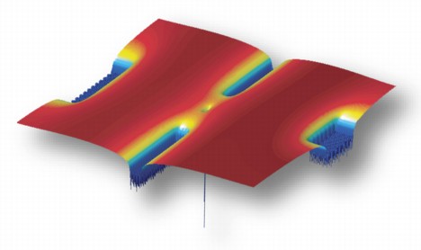
Simulations of the atomic transistor to model its behavior were conducted at Purdue using nanoHUB technology, an online community resource site for researchers in computational nanotechnology.
Gerhard Klimeck, who directed the Purdue group that ran the simulations, says this is an important development because it shows how small electronic components can be engineered.
"To me, this is the physical limit of Moore's Law," Klimeck says. "We can't make it smaller than this."
Although definitions can vary, simply stated Moore's Law holds that the number of transistors that can be placed on a processor will double approximately every 18 months. The latest Intel chip, the "Sandy Bridge," uses a manufacturing process to place 2.3 billion transistors 32 nanometers apart. A single phosphorus atom, by comparison, is just 0.1 nanometers across, which would significantly reduce the size of processors made using this technique, although it may be many years before single-atom processors actually are manufactured.
The single-atom transistor does have one serious limitation: It must be kept very cold, at least as cold as liquid nitrogen, or minus 391 degrees Fahrenheit (minus 196 Celsius).
"The atom sits in a well or channel, and for it to operate as a transistor the electrons must stay in that channel," Klimeck says. "At higher temperatures, the electrons move more and go outside of the channel. For this atom to act like a metal you have to contain the electrons to the channel.
"If someone develops a technique to contain the electrons, this technique could be used to build a computer that would work at room temperature. But this is a fundamental question for this technology."
Although single atoms serving as transistors have been observed before, this is the first time a single-atom transistor has been controllably engineered with atomic precision. The structure even has markers that allow researchers to attach contacts and apply a voltage, says Martin Fuechsle, a researcher at the University of New South Wales and lead author on the journal paper.
"The thing that is unique about what we have done is that we have, with atomic precision, positioned this individual atom within our device," Fuechsle says.
Simmons says this control is the key step in making a single-atom device. "By achieving the placement of a single atom, we have, at the same time, developed a technique that will allow us to be able to place several of these single-atom devices towards the goal of a developing a scalable system."
The single-atom transistor could lead the way to building a quantum computer that works by controlling the electrons and thereby the quantum information, or qubits. Some scientists, however, have doubts that such a device can ever be built.
"Whilst this result is a major milestone in scalable silicon quantum computing, it does not answer the question of whether quantum computing is possible or not," Simmons says. "The answer to this lies in whether quantum coherence can be controlled over large numbers of qubits. The technique we have developed is potentially scalable, using the same materials as the silicon industry, but more time is needed to realize this goal."
Klimeck says despite the hurdles, the single-atom transistor is an important development.
"This opens eyes because it is a device that behaves like metal in silicon. This will lead to many more discoveries."
The research project spanned the globe and was the result of many years of effort.
"When I established this program 10 years ago, many people thought it was impossible with too many technical hurdles. However, on reading into the literature I could not see any practical reason why it would not be possible," Simmons says. "Brute determination and systemic studies were necessary - as well as having many outstanding students and postdoctoral researchers who have worked on the project."
Klimeck notes that modern collaboration and community-building tools such as nanoHUB played an important role.
"This was a trans-Pacific collaboration that came about through the community created in nanoHUB. Now Purdue graduate students spend time studying at the University of New South Wales, and their students travel to Purdue to learn more about nanotechnology. It has been a rewarding collaboration, both for the scientific discoveries and for the personal relationships that were formed."
####
For more information, please click here
Contacts:
Writer:
Steve Tally
765-494-9809
Twitter: sciencewriter
Sources:
Michelle Simmons
0425 336 756
Gerhard Klimeck
765-494-9212
University of New South Wales media contact:
Mary O'Malley
0438 881 124
Copyright © Purdue University
If you have a comment, please Contact us.Issuers of news releases, not 7th Wave, Inc. or Nanotechnology Now, are solely responsible for the accuracy of the content.
Bookmark:


| Related Links |
![]() Down to the wire for silicon: Researchers create a wire 4 atoms wide, 1 atom tall:
Down to the wire for silicon: Researchers create a wire 4 atoms wide, 1 atom tall:
![]() University of New South Wales Centre for Quantum Computation & Communication Technology:
University of New South Wales Centre for Quantum Computation & Communication Technology:
| Related News Press |
News and information
![]() Quantum computer improves AI predictions April 17th, 2026
Quantum computer improves AI predictions April 17th, 2026
![]() Flexible sensor gains sensitivity under pressure April 17th, 2026
Flexible sensor gains sensitivity under pressure April 17th, 2026
![]() A reusable chip for particulate matter sensing April 17th, 2026
A reusable chip for particulate matter sensing April 17th, 2026
![]() Detecting vibrational quantum beating in the predissociation dynamics of SF6 using time-resolved photoelectron spectroscopy April 17th, 2026
Detecting vibrational quantum beating in the predissociation dynamics of SF6 using time-resolved photoelectron spectroscopy April 17th, 2026
Videos/Movies
![]() ICFO researchers overcome long-standing bottleneck in single photon detection with twisted 2D materials August 8th, 2025
ICFO researchers overcome long-standing bottleneck in single photon detection with twisted 2D materials August 8th, 2025
![]() New X-ray imaging technique to study the transient phases of quantum materials December 29th, 2022
New X-ray imaging technique to study the transient phases of quantum materials December 29th, 2022
![]() Solvent study solves solar cell durability puzzle: Rice-led project could make perovskite cells ready for prime time September 23rd, 2022
Solvent study solves solar cell durability puzzle: Rice-led project could make perovskite cells ready for prime time September 23rd, 2022
![]() Scientists prepare for the world�s smallest race: Nanocar Race II March 18th, 2022
Scientists prepare for the world�s smallest race: Nanocar Race II March 18th, 2022
Govt.-Legislation/Regulation/Funding/Policy
![]() Quantum computer improves AI predictions April 17th, 2026
Quantum computer improves AI predictions April 17th, 2026
![]() Metasurfaces smooth light to boost magnetic sensing precision January 30th, 2026
Metasurfaces smooth light to boost magnetic sensing precision January 30th, 2026
![]() New imaging approach transforms study of bacterial biofilms August 8th, 2025
New imaging approach transforms study of bacterial biofilms August 8th, 2025
Chip Technology
![]() A reusable chip for particulate matter sensing April 17th, 2026
A reusable chip for particulate matter sensing April 17th, 2026
![]() Metasurfaces smooth light to boost magnetic sensing precision January 30th, 2026
Metasurfaces smooth light to boost magnetic sensing precision January 30th, 2026
Quantum Computing
![]() Quantum computer improves AI predictions April 17th, 2026
Quantum computer improves AI predictions April 17th, 2026
![]() UC Irvine physicists discover method to reverse �quantum scrambling� : The work addresses the problem of information loss in quantum computing system April 17th, 2026
UC Irvine physicists discover method to reverse �quantum scrambling� : The work addresses the problem of information loss in quantum computing system April 17th, 2026
![]() Researchers develop molecular qubits that communicate at telecom frequencies October 3rd, 2025
Researchers develop molecular qubits that communicate at telecom frequencies October 3rd, 2025
Nanoelectronics
![]() Lab to industry: InSe wafer-scale breakthrough for future electronics August 8th, 2025
Lab to industry: InSe wafer-scale breakthrough for future electronics August 8th, 2025
![]() Interdisciplinary: Rice team tackles the future of semiconductors Multiferroics could be the key to ultralow-energy computing October 6th, 2023
Interdisciplinary: Rice team tackles the future of semiconductors Multiferroics could be the key to ultralow-energy computing October 6th, 2023
![]() Key element for a scalable quantum computer: Physicists from Forschungszentrum J�lich and RWTH Aachen University demonstrate electron transport on a quantum chip September 23rd, 2022
Key element for a scalable quantum computer: Physicists from Forschungszentrum J�lich and RWTH Aachen University demonstrate electron transport on a quantum chip September 23rd, 2022
![]() Reduced power consumption in semiconductor devices September 23rd, 2022
Reduced power consumption in semiconductor devices September 23rd, 2022
Discoveries
![]() Quantum computer improves AI predictions April 17th, 2026
Quantum computer improves AI predictions April 17th, 2026
![]() Flexible sensor gains sensitivity under pressure April 17th, 2026
Flexible sensor gains sensitivity under pressure April 17th, 2026
![]() A reusable chip for particulate matter sensing April 17th, 2026
A reusable chip for particulate matter sensing April 17th, 2026
![]() Detecting vibrational quantum beating in the predissociation dynamics of SF6 using time-resolved photoelectron spectroscopy April 17th, 2026
Detecting vibrational quantum beating in the predissociation dynamics of SF6 using time-resolved photoelectron spectroscopy April 17th, 2026
Announcements
![]() A fundamentally new therapeutic approach to cystic fibrosis: Nanobody repairs cellular defect April 17th, 2026
A fundamentally new therapeutic approach to cystic fibrosis: Nanobody repairs cellular defect April 17th, 2026
![]() UC Irvine physicists discover method to reverse �quantum scrambling� : The work addresses the problem of information loss in quantum computing system April 17th, 2026
UC Irvine physicists discover method to reverse �quantum scrambling� : The work addresses the problem of information loss in quantum computing system April 17th, 2026
Research partnerships
![]() Lab to industry: InSe wafer-scale breakthrough for future electronics August 8th, 2025
Lab to industry: InSe wafer-scale breakthrough for future electronics August 8th, 2025
![]() HKU physicists uncover hidden order in the quantum world through deconfined quantum critical points April 25th, 2025
HKU physicists uncover hidden order in the quantum world through deconfined quantum critical points April 25th, 2025
Quantum nanoscience
![]() Beyond silicon: Electronics at the scale of a single molecule January 30th, 2026
Beyond silicon: Electronics at the scale of a single molecule January 30th, 2026
![]() MXene nanomaterials enter a new dimension Multilayer nanomaterial: MXene flakes created at Drexel University show new promise as 1D scrolls January 30th, 2026
MXene nanomaterials enter a new dimension Multilayer nanomaterial: MXene flakes created at Drexel University show new promise as 1D scrolls January 30th, 2026
![]() ICFO researchers overcome long-standing bottleneck in single photon detection with twisted 2D materials August 8th, 2025
ICFO researchers overcome long-standing bottleneck in single photon detection with twisted 2D materials August 8th, 2025
|
|
||
|
|
||
| The latest news from around the world, FREE | ||
|
|
||
|
|
||
| Premium Products | ||
|
|
||
|
Only the news you want to read!
Learn More |
||
|
|
||
|
Full-service, expert consulting
Learn More |
||
|
|
||