Home > Press > CEA-Leti Launches Open 3D™ Initiative: New Global Offer Includes Design, Layout, Testing and Packaging on Leti Platforms
 |
Abstract:
CEA-Leti today announced the launch of a major new platform that provides industrial and academic partners with a global offer of mature 3D innovative technologies for their advanced products and research projects.
CEA-Leti Launches Open 3D™ Initiative: New Global Offer Includes Design, Layout, Testing and Packaging on Leti Platforms
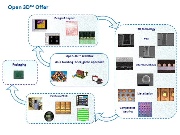
Grenoble, France | Posted on January 31st, 2012To help its partners solve key technology challenges, Leti's Open 3D™ global offer includes 3D design, layout, technologies including interconnections, TSV and components assembly, reliability tests and final packaging for components or systems achievement.
The Open 3D™ platform includes Leti's proven "off-the-shelf" 3D technologies that provides decisive advantages in performance, form factor and cost for a wide range of markets like bio/medical, aeronautics and space, consumer applications, defense and security, or fundamental research.
The platform enables customers to achieve proof of concept with a small quantity of wafers or prototyping with a larger quantity. The offer is based on limited mature technologies in order to ensure moderate costs, short cycle times and performances corresponding to the initial technical requirements of Leti customers.
Open 3D™ also operates directly on active wafers with embedded components or on passive wafers for interposer technologies.
"Open 3D leverages Leti's proven 3D expertise and infrastructure for collaborations that address new applications and markets, as a key new part of Leti's mission to create innovation and transfer it to industry," said Laurent Malier, CEO of Leti. "Our partners will include laboratories, universities and international research institutes as well as fabless chip companies and niche market manufacturers and integrators."
Operated on the Minatec Campus in Grenoble with Leti teams and technological platforms, Open 3D™ is fully operational for 200mm wafers and will be operational in 2012 for 300mm wafers. Modules offered in the platform's technology catalogue include:
- Through silicon vias (TSV) with aspect ratios to 1:3
- Interconnects for chips to wafers based on micro-bumps technology
- Interconnects for chips to substrates based on bumps technology
- Redistribution layers (RDL)
- Under-bump metallurgy (UBM)
- Temporary bonding, thinning and debonding
The technology catalogue will be regularly enriched with new technological modules that correspond with new 3D mature technologies and customer requirements.
####
About CEA-Leti
CEA is a French research and technology organization, with activities in four main areas: energy, information technologies, healthcare technologies and defence and security. Within CEA, the Laboratory for Electronics & Information Technology (CEA-Leti) works with companies in order to increase their competitiveness through technological innovation and transfers. CEA-Leti is focused on micro and nanotechnologies and their applications, from wireless devices and systems, to biology and healthcare or photonics. Nanoelectronics and microsystems (MEMS) are at the core of its activities. As a major player in MINATEC campus, CEA-Leti operates 8,000-m˛ state-of-the-art clean rooms, on 24/7 mode, on 200mm and 300mm wafer standards. With 1,400 employees, CEA-Leti trains more than 190 Ph.D. students and hosts 200 assignees from partner companies. Strongly committed to the creation of value for the industry, CEA-Leti puts a strong emphasis on intellectual property and owns more than 1,700 patent families.
Visit www.leti.fr.
For more information, please click here
Contacts:
Technical contact:
CEA-Leti
David Henry
+33 4 38 78 96 88
Media Contact:
CEA-Leti
Thierry Bosc
+33 4 38 78 31 95
Weber Shandwick
Eric Chauvelot / Robert Ba
+33 1 47 59 56 57 / 38 75
Copyright © CEA-Leti
If you have a comment, please Contact us.Issuers of news releases, not 7th Wave, Inc. or Nanotechnology Now, are solely responsible for the accuracy of the content.
Bookmark:


| Related News Press |
News and information
![]() Simulating magnetization in a Heisenberg quantum spin chain April 5th, 2024
Simulating magnetization in a Heisenberg quantum spin chain April 5th, 2024
![]() NRL charters Navy’s quantum inertial navigation path to reduce drift April 5th, 2024
NRL charters Navy’s quantum inertial navigation path to reduce drift April 5th, 2024
![]() Discovery points path to flash-like memory for storing qubits: Rice find could hasten development of nonvolatile quantum memory April 5th, 2024
Discovery points path to flash-like memory for storing qubits: Rice find could hasten development of nonvolatile quantum memory April 5th, 2024
Chip Technology
![]() Discovery points path to flash-like memory for storing qubits: Rice find could hasten development of nonvolatile quantum memory April 5th, 2024
Discovery points path to flash-like memory for storing qubits: Rice find could hasten development of nonvolatile quantum memory April 5th, 2024
![]() Utilizing palladium for addressing contact issues of buried oxide thin film transistors April 5th, 2024
Utilizing palladium for addressing contact issues of buried oxide thin film transistors April 5th, 2024
![]() HKUST researchers develop new integration technique for efficient coupling of III-V and silicon February 16th, 2024
HKUST researchers develop new integration technique for efficient coupling of III-V and silicon February 16th, 2024
Nanoelectronics
![]() Interdisciplinary: Rice team tackles the future of semiconductors Multiferroics could be the key to ultralow-energy computing October 6th, 2023
Interdisciplinary: Rice team tackles the future of semiconductors Multiferroics could be the key to ultralow-energy computing October 6th, 2023
![]() Key element for a scalable quantum computer: Physicists from Forschungszentrum Jülich and RWTH Aachen University demonstrate electron transport on a quantum chip September 23rd, 2022
Key element for a scalable quantum computer: Physicists from Forschungszentrum Jülich and RWTH Aachen University demonstrate electron transport on a quantum chip September 23rd, 2022
![]() Reduced power consumption in semiconductor devices September 23rd, 2022
Reduced power consumption in semiconductor devices September 23rd, 2022
![]() Atomic level deposition to extend Moore’s law and beyond July 15th, 2022
Atomic level deposition to extend Moore’s law and beyond July 15th, 2022
Announcements
![]() NRL charters Navy’s quantum inertial navigation path to reduce drift April 5th, 2024
NRL charters Navy’s quantum inertial navigation path to reduce drift April 5th, 2024
![]() Discovery points path to flash-like memory for storing qubits: Rice find could hasten development of nonvolatile quantum memory April 5th, 2024
Discovery points path to flash-like memory for storing qubits: Rice find could hasten development of nonvolatile quantum memory April 5th, 2024
Alliances/Trade associations/Partnerships/Distributorships
![]() Chicago Quantum Exchange welcomes six new partners highlighting quantum technology solutions, from Chicago and beyond September 23rd, 2022
Chicago Quantum Exchange welcomes six new partners highlighting quantum technology solutions, from Chicago and beyond September 23rd, 2022
![]() University of Illinois Chicago joins Brookhaven Lab's Quantum Center June 10th, 2022
University of Illinois Chicago joins Brookhaven Lab's Quantum Center June 10th, 2022
|
|
||
|
|
||
| The latest news from around the world, FREE | ||
|
|
||
|
|
||
| Premium Products | ||
|
|
||
|
Only the news you want to read!
Learn More |
||
|
|
||
|
Full-service, expert consulting
Learn More |
||
|
|
||