Home > Press > Compact, low-cost and fast hyperspectral imaging solution
 |
Abstract:
Today at SPIE Photonics West 2012, imec has demonstrated a hyperspectral camera solution based on a system-on-chip image sensor with an integrated hyperspectral sensor. Imec's solution is fast and enables small and cost-efficient camera-solutions. It targets multiple industrial vision applications.
Compact, low-cost and fast hyperspectral imaging solution
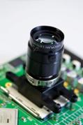
San Francisco, CA and Leuven, Belgium | Posted on January 24th, 2012Hyperspectral cameras combine spectroscopy and imaging, and by doing this, they can e.g. discriminate between different objects that cannot be accurately distinguished using traditional RGB (red-green-blue) imaging methods. The technology can be very useful in many application domains such as crop screening, food selection, skin cancer detection, target detection, .... However, the currently available hyperspectral cameras are large, expensive and slow. Therefore, they can often not be used for time-critical or high-throughput applications, and their use is thus limited to highly specialized research environments. Imec's chip-based technology paves the way towards the industrial application of hyperspectral imaging, as it enables small, cost-efficient and fast solutions.
Imec's fully integrated CMOS compatible hyperspectral sensor, today presented at SPIE Photonics West 2012, consists of a set of spectral filters that are directly post-processed at wafer level on top of a commercially available CMOSIS CMV4000 image sensor (a 4 megapixel sensor with a maximum framerate of 180fps). The hyperspectral filter, developed at imec, has100 spectral bands between 560nm and 1000nm. The filter bandwidth (Full Width Half Max) ranges from 3nm at 560nm to 20nm at 1000nm, and the transmission efficiency of the filters is around 85%. Typical integration times used in the current prototype setup are between 2 and 10 miliseconds under halogen light illumination of 450 Watt. This indicates maximal frame rates can be achieved of up to 500fp.
Due to its integrated filter design and high spectral filter efficiency, imec's solution can obtain scanning speeds that are compatible with real industrial requirements. The speed of the demonstrated system corresponds to an equivalent speed of 2,000 lines per second, significantly exceeding current state-of-the-art hyperspectral sensors. Moreover, imec's technology can be adopted to a range of industrial vision applications. To match to specific application requirements, the image sensor can be selected (a commercially available sensor or even a custom-designed sensor), determining pixels sizes, maximal frame rate, etc. The hyperspectral filter can be tuned by changing the number of spectral bands and their spectral resolution.
Imec's prototype hyperspectral camera can capture all relevant data enabling automatic classification of different objects using state-of-the-art image processing methods. Classification results of imec's solution are equivalent to state-of-the-art hyperspectral references and recorded spectra of, for example, plant material.
####
About IMEC
Imec performs world-leading research in nanoelectronics. Imec leverages its scientific knowledge with the innovative power of its global partnerships in ICT, healthcare and energy. Imec delivers industry-relevant technology solutions. In a unique high-tech environment, its international top talent is committed to providing the building blocks for a better life in a sustainable society. Imec is headquartered in Leuven, Belgium, and has offices in Belgium, the Netherlands, Taiwan, US, China, India and Japan. Its staff of about 1,900 people includes more than 500 industrial residents and guest researchers. In 2010, imec's revenue (P&L) was 285 million euro. Further information on imec can be found at www.imec.be.
Imec is a registered trademark for the activities of IMEC International (a legal entity set up under Belgian law as a "stichting van openbaar nut�), imec Belgium (IMEC vzw supported by the Flemish Government), imec the Netherlands (Stichting IMEC Nederland, part of Holst Centre which is supported by the Dutch Government), imec Taiwan (IMEC Taiwan Co.) and imec China (IMEC Microelectronics (Shangai) Co. Ltd.) and imec India (Imec India Private Limited).
For more information, please click here
Contacts:
Hanne Degans
External Communications Officer
T: +32 16 28 17 69
Mobile: +32 486 065 175
Barbara Kalkis
Maestro Marketing & PR
T: +1 408 996 9975
M: +1 408 529 4210
Copyright © IMEC
If you have a comment, please Contact us.Issuers of news releases, not 7th Wave, Inc. or Nanotechnology Now, are solely responsible for the accuracy of the content.
Bookmark:


| Related News Press |
News and information
![]() Simulating magnetization in a Heisenberg quantum spin chain April 5th, 2024
Simulating magnetization in a Heisenberg quantum spin chain April 5th, 2024
![]() NRL charters Navy�s quantum inertial navigation path to reduce drift April 5th, 2024
NRL charters Navy�s quantum inertial navigation path to reduce drift April 5th, 2024
![]() Discovery points path to flash-like memory for storing qubits: Rice find could hasten development of nonvolatile quantum memory April 5th, 2024
Discovery points path to flash-like memory for storing qubits: Rice find could hasten development of nonvolatile quantum memory April 5th, 2024
Imaging
![]() Nanoscale CL thermometry with lanthanide-doped heavy-metal oxide in TEM March 8th, 2024
Nanoscale CL thermometry with lanthanide-doped heavy-metal oxide in TEM March 8th, 2024
![]() The USTC realizes In situ electron paramagnetic resonance spectroscopy using single nanodiamond sensors November 3rd, 2023
The USTC realizes In situ electron paramagnetic resonance spectroscopy using single nanodiamond sensors November 3rd, 2023
![]() Observation of left and right at nanoscale with optical force October 6th, 2023
Observation of left and right at nanoscale with optical force October 6th, 2023
Announcements
![]() NRL charters Navy�s quantum inertial navigation path to reduce drift April 5th, 2024
NRL charters Navy�s quantum inertial navigation path to reduce drift April 5th, 2024
![]() Discovery points path to flash-like memory for storing qubits: Rice find could hasten development of nonvolatile quantum memory April 5th, 2024
Discovery points path to flash-like memory for storing qubits: Rice find could hasten development of nonvolatile quantum memory April 5th, 2024
Tools
![]() Ferroelectrically modulate the Fermi level of graphene oxide to enhance SERS response November 3rd, 2023
Ferroelectrically modulate the Fermi level of graphene oxide to enhance SERS response November 3rd, 2023
![]() The USTC realizes In situ electron paramagnetic resonance spectroscopy using single nanodiamond sensors November 3rd, 2023
The USTC realizes In situ electron paramagnetic resonance spectroscopy using single nanodiamond sensors November 3rd, 2023
Events/Classes
![]() Researchers demonstrate co-propagation of quantum and classical signals: Study shows that quantum encryption can be implemented in existing fiber networks January 20th, 2023
Researchers demonstrate co-propagation of quantum and classical signals: Study shows that quantum encryption can be implemented in existing fiber networks January 20th, 2023
|
|
||
|
|
||
| The latest news from around the world, FREE | ||
|
|
||
|
|
||
| Premium Products | ||
|
|
||
|
Only the news you want to read!
Learn More |
||
|
|
||
|
Full-service, expert consulting
Learn More |
||
|
|
||