Home > Press > Biocompatible graphene transistor array reads cellular signals: Novel nanocarbon platform shows potential for future bioelectronic implants
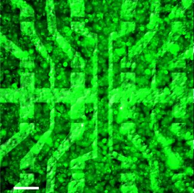 |
| This combination of optical microscopy and fluorescence imaging shows a layer of biological cells covering a graphene-based transistor array. The experimental device, created by scientists from the Technische Universitaet Muenchen and the Juelich Research Center, is the first of its kind to prove capable of recording signals generated by living cells, with good spatial and temporal resolution. With this demonstration, the researchers have opened the way to further investigation of the feasibility of using graphene-based bioelectronics for potential future applications such as neuroprosthetic implants in the brain, the eye, or the ear.
Credit: Copyright TU Muenchen |
Abstract:
Researchers have demonstrated, for the first time, a graphene-based transistor array that is compatible with living biological cells and capable of recording the electrical signals they generate. This proof-of-concept platform opens the way for further investigation of a promising new material. Graphene's distinctive combination of characteristics makes it a leading contender for future biomedical applications requiring a direct interface between microelectronic devices and nerve cells or other living tissue. A team of scientists from the Technische Universitaet Muenchen and the Juelich Research Center published the results in the journal Advanced Materials.
Biocompatible graphene transistor array reads cellular signals: Novel nanocarbon platform shows potential for future bioelectronic implants
Garching, Germany | Posted on November 30th, 2011Today, if a person has an intimate and dependent relationship with an electronic device, it's most likely to be a smart phone; however, much closer connections may be in store in the foreseeable future. For example, "bioelectronic" applications have been proposed that would place sensors and in some cases actuators inside a person's brain, eye, or ear to help compensate for neural damage. Pioneering research in this direction was done using the mature technology of silicon microelectronics, but in practice that approach may be a dead end: Both flexible substrates and watery biological environments pose serious problems for silicon devices; in addition, they may be too "noisy" for reliable communication with individual nerve cells.
Of the several material systems being explored as alternatives, graphene - essentially a two-dimensional sheet of carbon atoms linked in a dense honeycomb pattern - seems very well suited to bioelectronic applications: It offers outstanding electronic performance, is chemically stable and biologically inert, can readily be processed on flexible substrates, and should lend itself to large-scale, low-cost fabrication. The latest results from the TUM-Juelich team confirm key performance characteristics and open the way for further advances toward determining the feasibility of graphene-based bioelectronics.
The experimental setup reported in Advanced Materials began with an array of 16 graphene solution-gated field-effect transistors (G-SGFETs) fabricated on copper foil by chemical vapor deposition and standard photolithographic and etching processes. "The sensing mechanism of these devices is rather simple," says Dr. Jose Antonio Garrido, a member of the Walter Schottky Institute at TUM. "Variations of the electrical and chemical environment in the vicinity of the FET gate region will be converted into a variation of the transistor current."
Directly on top of this array, the researchers grew a layer of biological cells similar to heart muscle. Not only were the "action potentials" of individual cells detectable above the intrinsic electrical noise of the transistors, but these cellular signals could be recorded with high spatial and temporal resolution. For example, a series of spikes separated by tens of milliseconds moved across the transistor array in just the way action potentials could be expected to propagate across the cell layer. Also, when the cell layer was exposed to a higher concentration of the stress hormone norepinephrine, a corresponding increase in the frequency of spikes was recorded. Separate experiments to determine the inherent noise level of the G-SFETs showed it to be comparable to that of ultralow-noise silicon devices, which as Garrido points out are the result of decades of technological development.
"Much of our ongoing research is focused on further improving the noise performance of graphene devices," Garrido says, "and on optimizing the transfer of this technology to flexible substrates such as parylene and kapton, both of which are currently used for in vivo implants. We are also working to improve the spatial resolution of our recording devices." Meanwhile, they are working with scientists at the Paris-based Vision Institute to investigate the biocompatibility of graphene layers in cultures of retinal neuron cells, as well as within a broader European project called NEUROCARE, which aims at developing brain implants based on flexible nanocarbon devices.
This research is supported by the German Research Foundation (DFG) within Priority Program 1459 "Graphene," the International Helmholtz Research School BioSoft, the Bavarian Graduate School CompInt, the TUM Institute for Advanced Study, and the Nanosystems Initiative Munich (NIM).
Original publication: Graphene Transistor Arrays for Recording Action Potentials from Electrogenic Cells; Lucas H. Hess, Michael Jansen, Vanessa Maybeck, Moritz V. Hauf, Max Seifert, Martin Stutzmann, Ian D. Sharp, Andreas Offenhaeusser, and Jose A. Garrido. Advanced Materials 2011, 23, 5045-5049. DOI: 10.1002/adma.201102990.
####
About Technische Universitaet Muenchen
Technische Universitaet Muenchen (TUM) is one of Europe's leading universities. It has roughly 460 professors, 9000 academic and non-academic staff, and 31,500 students. It focuses on the engineering sciences, natural sciences, life sciences, medicine, and economic sciences. After winning numerous awards, it was selected as an "Elite University" in 2006 by the Science Council (Wissenschaftsrat) and the German Research Foundation (DFG). The university's global network includes an outpost with a research campus in Singapore. TUM is dedicated to the ideal of a top-level research-based entrepreneurial university.
For more information, please click here
Contacts:
Patrick Regan
49-892-891-0515
Dr. J. A. Garrido
Walter Schottky Institute
Technische Universitaet Muenchen
Am Coulombwall 4
85748 Garching, Germany
Tel: +49 89 289 12766
E-mail:
Home page: www.wsi.tum.de
Copyright © Technische Universitaet Muenchen
If you have a comment, please Contact us.Issuers of news releases, not 7th Wave, Inc. or Nanotechnology Now, are solely responsible for the accuracy of the content.
Bookmark:


| Related News Press |
News and information
![]() Simulating magnetization in a Heisenberg quantum spin chain April 5th, 2024
Simulating magnetization in a Heisenberg quantum spin chain April 5th, 2024
![]() NRL charters Navy�s quantum inertial navigation path to reduce drift April 5th, 2024
NRL charters Navy�s quantum inertial navigation path to reduce drift April 5th, 2024
![]() Discovery points path to flash-like memory for storing qubits: Rice find could hasten development of nonvolatile quantum memory April 5th, 2024
Discovery points path to flash-like memory for storing qubits: Rice find could hasten development of nonvolatile quantum memory April 5th, 2024
Imaging
![]() Nanoscale CL thermometry with lanthanide-doped heavy-metal oxide in TEM March 8th, 2024
Nanoscale CL thermometry with lanthanide-doped heavy-metal oxide in TEM March 8th, 2024
Graphene/ Graphite
![]() NRL discovers two-dimensional waveguides February 16th, 2024
NRL discovers two-dimensional waveguides February 16th, 2024
Brain-Computer Interfaces
![]() Taking salt out of the water equation October 7th, 2022
Taking salt out of the water equation October 7th, 2022
![]() New brain-like computing device simulates human learning: Researchers conditioned device to learn by association, like Pavlov's dog April 30th, 2021
New brain-like computing device simulates human learning: Researchers conditioned device to learn by association, like Pavlov's dog April 30th, 2021
Chip Technology
![]() Discovery points path to flash-like memory for storing qubits: Rice find could hasten development of nonvolatile quantum memory April 5th, 2024
Discovery points path to flash-like memory for storing qubits: Rice find could hasten development of nonvolatile quantum memory April 5th, 2024
![]() Utilizing palladium for addressing contact issues of buried oxide thin film transistors April 5th, 2024
Utilizing palladium for addressing contact issues of buried oxide thin film transistors April 5th, 2024
![]() HKUST researchers develop new integration technique for efficient coupling of III-V and silicon February 16th, 2024
HKUST researchers develop new integration technique for efficient coupling of III-V and silicon February 16th, 2024
Nanomedicine
![]() New micromaterial releases nanoparticles that selectively destroy cancer cells April 5th, 2024
New micromaterial releases nanoparticles that selectively destroy cancer cells April 5th, 2024
![]() Good as gold - improving infectious disease testing with gold nanoparticles April 5th, 2024
Good as gold - improving infectious disease testing with gold nanoparticles April 5th, 2024
![]() Researchers develop artificial building blocks of life March 8th, 2024
Researchers develop artificial building blocks of life March 8th, 2024
Discoveries
![]() Chemical reactions can scramble quantum information as well as black holes April 5th, 2024
Chemical reactions can scramble quantum information as well as black holes April 5th, 2024
![]() New micromaterial releases nanoparticles that selectively destroy cancer cells April 5th, 2024
New micromaterial releases nanoparticles that selectively destroy cancer cells April 5th, 2024
![]() Utilizing palladium for addressing contact issues of buried oxide thin film transistors April 5th, 2024
Utilizing palladium for addressing contact issues of buried oxide thin film transistors April 5th, 2024
Announcements
![]() NRL charters Navy�s quantum inertial navigation path to reduce drift April 5th, 2024
NRL charters Navy�s quantum inertial navigation path to reduce drift April 5th, 2024
![]() Discovery points path to flash-like memory for storing qubits: Rice find could hasten development of nonvolatile quantum memory April 5th, 2024
Discovery points path to flash-like memory for storing qubits: Rice find could hasten development of nonvolatile quantum memory April 5th, 2024
Tools
![]() Ferroelectrically modulate the Fermi level of graphene oxide to enhance SERS response November 3rd, 2023
Ferroelectrically modulate the Fermi level of graphene oxide to enhance SERS response November 3rd, 2023
![]() The USTC realizes In situ electron paramagnetic resonance spectroscopy using single nanodiamond sensors November 3rd, 2023
The USTC realizes In situ electron paramagnetic resonance spectroscopy using single nanodiamond sensors November 3rd, 2023
|
|
||
|
|
||
| The latest news from around the world, FREE | ||
|
|
||
|
|
||
| Premium Products | ||
|
|
||
|
Only the news you want to read!
Learn More |
||
|
|
||
|
Full-service, expert consulting
Learn More |
||
|
|
||