Home > Press > NT-MDT shares its SPM expertise
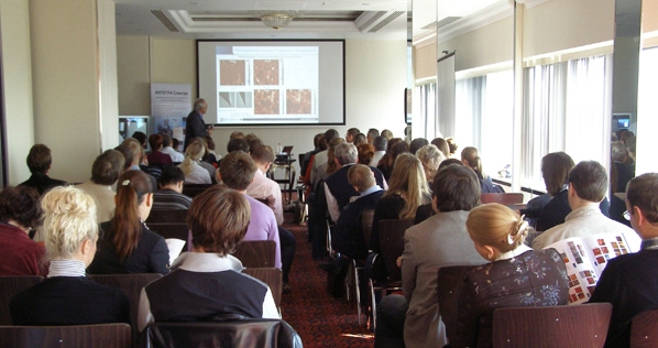 |
| At the workshop "Visualization of surfaces with the extreme resolution and study of local mechanical and electrical properties" in Russia. |
Abstract:
CEO of NT-MDT Development Dr. Sergei Magonov shared his comprehensive expertise on SPM techniques during scientific workshops in Russia and China.
NT-MDT shares its SPM expertise
Moscow, Russia and Shanghai, China | Posted on October 18th, 2011Dr. Sergey Magonov - a recognized authority of scanning probe microscopy and a world-wide renowned scientist - prepared a special scientific workshop "Visualization of surfaces with the extreme resolution and study of local mechanical and electrical properties".
During the workshop Dr. Magonov drew participants' attention to the detailed analysis of the possibilities and limitations of SPM as a methodical approach.
Practically receipt of the dependable data, which is necessary to precisely visualize the surface structure and to make an accurate quantitative analysis of local properties, is not an easy process and often can be more complex due to artifacts.
The solution to the problem includes rational choice of the probe, measuring method and optimal experimental parameters. Properly prepared and correctly conducted experiments considerably facilitates their analysis, especially taking into account the effect of the probe and level of the force interaction.
The first scientific workshop was held in early September in Shanghai (China). Afterwards it moved to Moscow (Russia) in the Institute of Crystallography (Russian Academy of Sciences). In both countries the workshops attracted keen interest of the audience. Totally over 150 people participated in the workshops.
NT-MDT intends to increase its efforts in developing a scientific basis of the SPM. We will continue to work with leading specialists in SPM and it's one of the most important directions of our management in the production of up-to-date equipment.
####
For more information, please click here
Contacts:
NT-MDT Co. Building 100
Zelenograd, Moscow 124482, Russia
Phone:+7 (499) 735-7777
Fax: +7 (499) 735-6410
Copyright © NT-MDT
If you have a comment, please Contact us.Issuers of news releases, not 7th Wave, Inc. or Nanotechnology Now, are solely responsible for the accuracy of the content.
Bookmark:


| Related News Press |
News and information
![]() Simulating magnetization in a Heisenberg quantum spin chain April 5th, 2024
Simulating magnetization in a Heisenberg quantum spin chain April 5th, 2024
![]() NRL charters Navy�s quantum inertial navigation path to reduce drift April 5th, 2024
NRL charters Navy�s quantum inertial navigation path to reduce drift April 5th, 2024
![]() Discovery points path to flash-like memory for storing qubits: Rice find could hasten development of nonvolatile quantum memory April 5th, 2024
Discovery points path to flash-like memory for storing qubits: Rice find could hasten development of nonvolatile quantum memory April 5th, 2024
Imaging
![]() Nanoscale CL thermometry with lanthanide-doped heavy-metal oxide in TEM March 8th, 2024
Nanoscale CL thermometry with lanthanide-doped heavy-metal oxide in TEM March 8th, 2024
![]() The USTC realizes In situ electron paramagnetic resonance spectroscopy using single nanodiamond sensors November 3rd, 2023
The USTC realizes In situ electron paramagnetic resonance spectroscopy using single nanodiamond sensors November 3rd, 2023
![]() Observation of left and right at nanoscale with optical force October 6th, 2023
Observation of left and right at nanoscale with optical force October 6th, 2023
Announcements
![]() NRL charters Navy�s quantum inertial navigation path to reduce drift April 5th, 2024
NRL charters Navy�s quantum inertial navigation path to reduce drift April 5th, 2024
![]() Discovery points path to flash-like memory for storing qubits: Rice find could hasten development of nonvolatile quantum memory April 5th, 2024
Discovery points path to flash-like memory for storing qubits: Rice find could hasten development of nonvolatile quantum memory April 5th, 2024
Tools
![]() Ferroelectrically modulate the Fermi level of graphene oxide to enhance SERS response November 3rd, 2023
Ferroelectrically modulate the Fermi level of graphene oxide to enhance SERS response November 3rd, 2023
![]() The USTC realizes In situ electron paramagnetic resonance spectroscopy using single nanodiamond sensors November 3rd, 2023
The USTC realizes In situ electron paramagnetic resonance spectroscopy using single nanodiamond sensors November 3rd, 2023
Events/Classes
![]() Researchers demonstrate co-propagation of quantum and classical signals: Study shows that quantum encryption can be implemented in existing fiber networks January 20th, 2023
Researchers demonstrate co-propagation of quantum and classical signals: Study shows that quantum encryption can be implemented in existing fiber networks January 20th, 2023
|
|
||
|
|
||
| The latest news from around the world, FREE | ||
|
|
||
|
|
||
| Premium Products | ||
|
|
||
|
Only the news you want to read!
Learn More |
||
|
|
||
|
Full-service, expert consulting
Learn More |
||
|
|
||